Multi-selective polishing slurry composition and a semiconductor element production method using the same

a technology of polishing slurry and slurry composition, which is applied in the direction of electrical equipment, chemical equipment and processes, other chemical processes, etc., can solve the problems of difficult to achieve overall planarization over the entire area of a semiconductor device, and difficult to ensure a lithography margin in the upper layer, so as to reduce the polishing rate of the insulating film and prevent over-polishing

Active Publication Date: 2015-06-25
IUCF HYU (IND UNIV COOP FOUND HANYANG UNIV)
View PDF3 Cites 1 Cited by
  • Summary
  • Abstract
  • Description
  • Claims
  • Application Information

AI Technical Summary

Benefits of technology

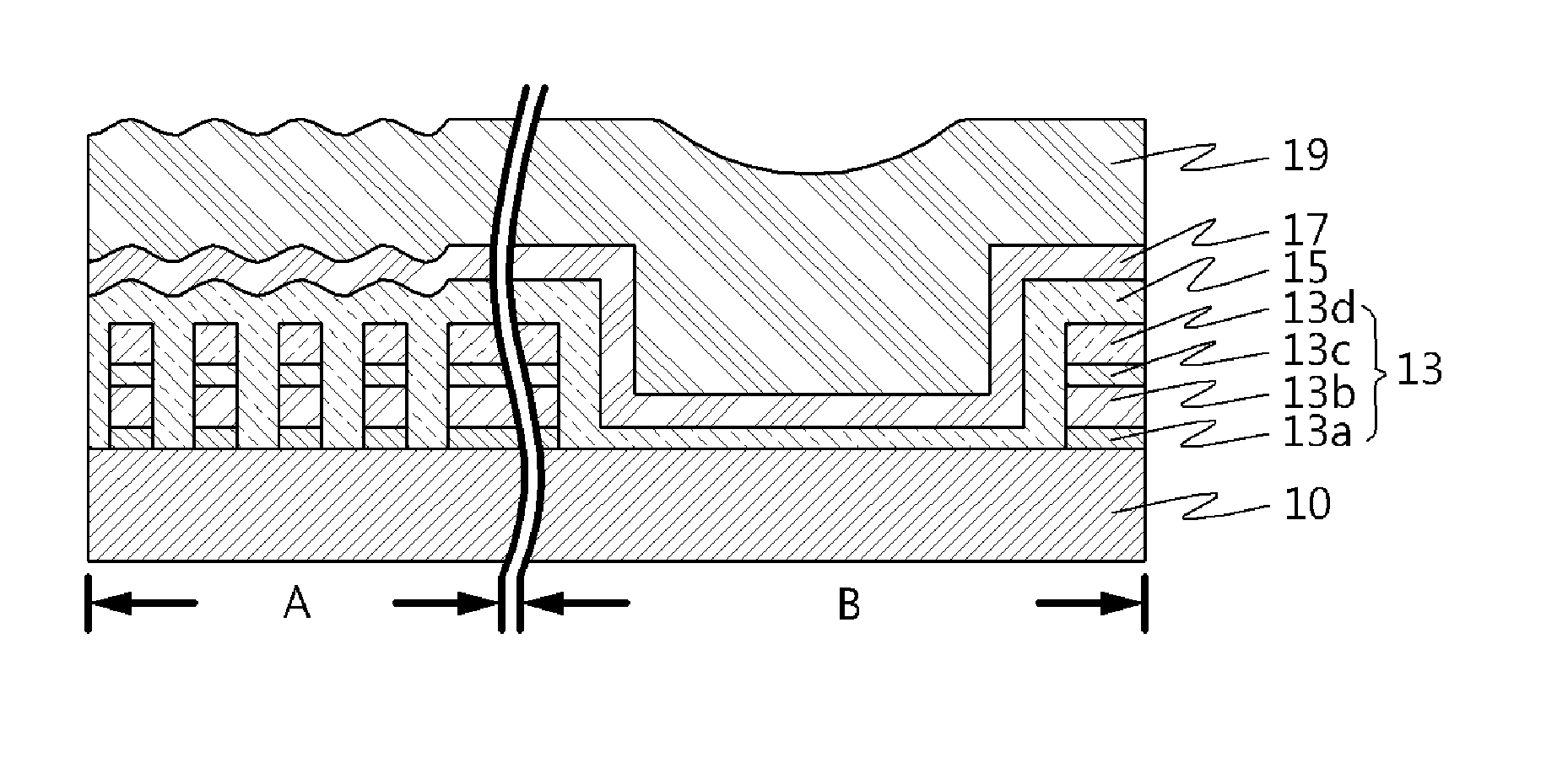
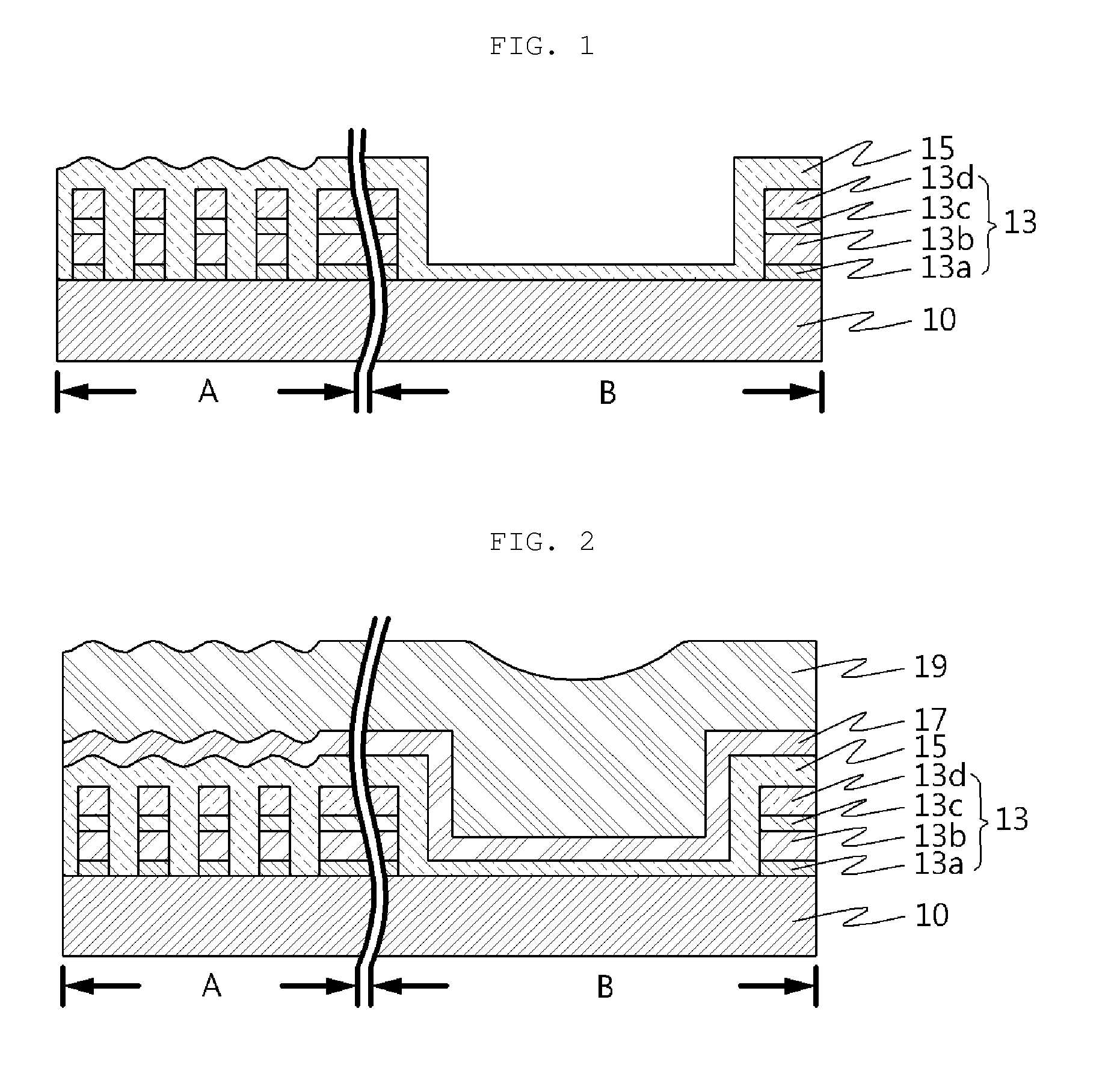
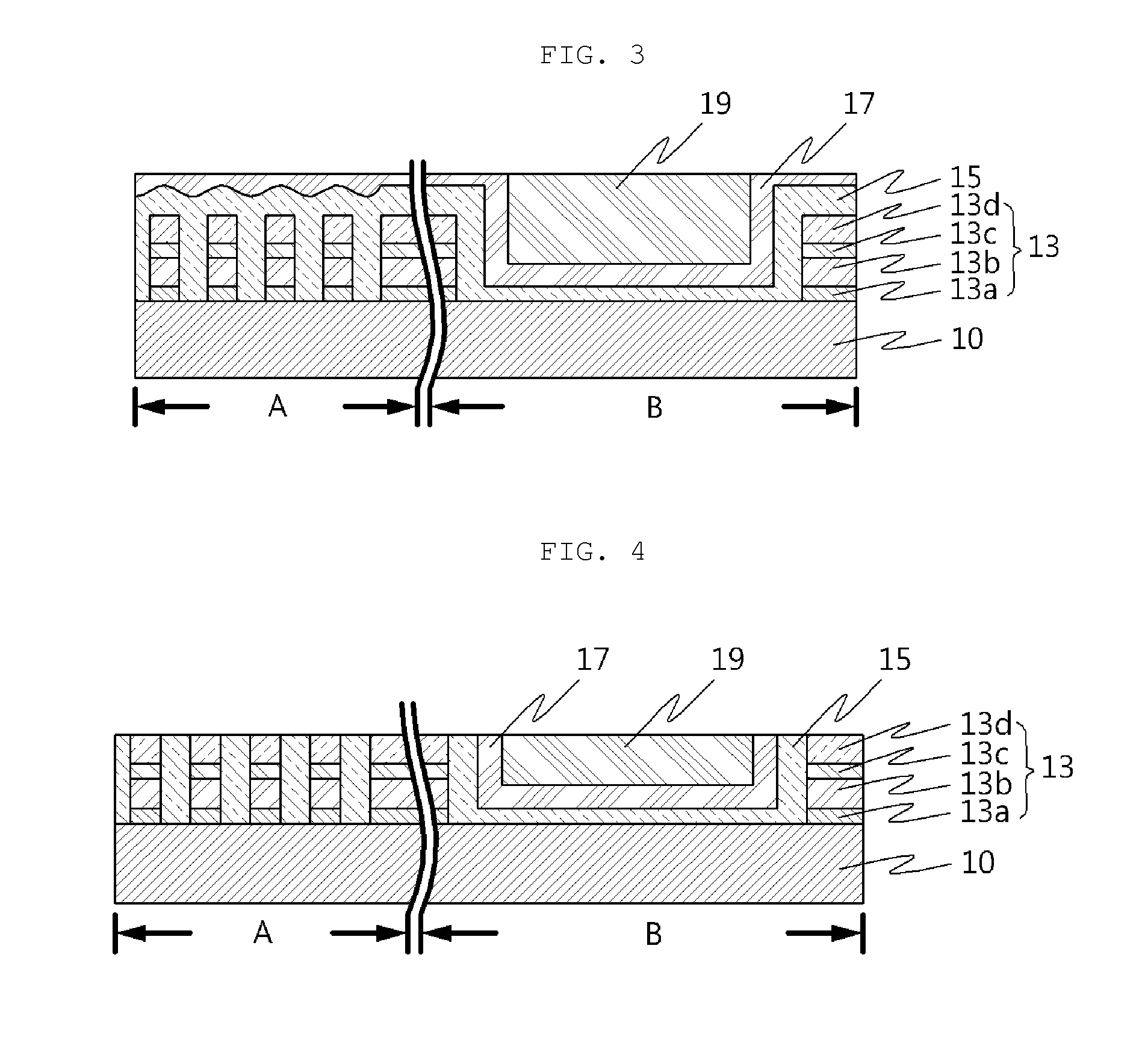
[0010]As described above, according to the present invention, a chemical mechanical polishing (CMP) process is performed using a polishing slurry composition containing a polishing agent, a silicon nitride film passivation agent, and a silicon film passivation agent. During the polishing process, the silicon nitride film passivation agent contained in the polishing slurring composition forms a passivation film on the silicon nitride film exposed on the first area, thereby reducing the polishing rate of the insulating film on the first area compared to the second area. Therefore, it is possible to prevent over-polishing in the first area in which the density of the device patterns is high, thereby forming a globally planarized surface. In other words, it is possible to primarily compensate for the pattern density effect of the device patterns.
[0011]Moreover, when the silicon film is exposed as the polishing process is further performed, the silicon film passivation agent contained in the polishing slurry composition forms a passivation film on the silicon film, thereby preventing the silicon film from being polished.

Problems solved by technology

When wirings having a very small line width are formed in multiple layers, it may be difficult to ensure a lithography margin in the upper layer.
However, even when applying the CMP process, it is difficult to achieve overall planarization over the entire area of a semiconductor device.
In this case, during the CMP process, the cell array area is over-polished due to high polishing rate, the peripheral circuit area is under-polished due to low polishing rate, and thus the planarization cannot be achieved over the entire area.
In this case, an error may occur during operation of the device.

Method used


Image

  • Multi-selective polishing slurry composition and a semiconductor element production method using the same
  • Multi-selective polishing slurry composition and a semiconductor element production method using the same
  • Multi-selective polishing slurry composition and a semiconductor element production method using the same

Examples


preparation example 1

of Polishing Slurry Composition

[0039]1,000 g of an additive solution was prepared by adding 0.01 parts by weight of poly(acrylic acid) (PAA) having a weight average molecular weight of 10,000 with respect to 100 parts by weight of deionized water. The additive solution was mixed with 1,000 g of a ceria suspension containing 5 wt % ceria particles and stirred. Then, 5,000 g of deionized water was added thereto to prepare a polishing slurry composition.

preparation example 2

of Polishing Slurry Composition

[0040]A polishing slurry composition was prepared in the same manner as Preparation Example 1, except that 0.05 parts by weight of poly(acrylic acid) (PAA) was added with respect to 100 parts by weight of deionized water.

preparation example 3

of Polishing Slurry Composition

[0041]A polishing slurry composition was prepared in the same manner as Preparation Example 1, except that 0.1 parts by weight of poly(acrylic acid) (PAA) was added with respect to 100 parts by weight of deionized water.


PUM

PropertyMeasurementUnit
densityaaaaaaaaaa
thicknessaaaaaaaaaa
weightaaaaaaaaaa

Abstract

Provided are a multi-selective polishing slurry composition and a semiconductor element production method using the same. A silicon film provided with element patterns is formed on the uppermost part of a substrate having a first region and a second region. The element pattern density on the first region is higher than the element pattern density on the second region. Formed in sequence on top of the element patterns are a first silicon oxide film, a silicon nitride film and a second silicon oxide film. The substrate is subjected to chemical-mechanical polishing until the silicon film is exposed, by using a polishing slurry composition containing a polishing agent, a silicon nitride film passivation agent and a silicon film passivation agent. The polishing slurry composition may be a mixture of 100 parts by weight of a polishing agent suspension, containing a polishing agent, and from 40 to 120 parts by weight of an additive solution, and the additive solution can contain 100 parts by weight of a solvent, from 0.01 to 5 parts by weight of a silicon nitride film passivation agent and from 0.01 to 5 parts by weight of a silicon film passivation agent.

Description

TECHNICAL FIELD[0001]The present invention relates to a polishing slurry composition and, more particularly, to a slurry composition for polishing an oxide film and a nitride film, and a method for producing a semiconductor device using the same.BACKGROUND ART[0002]Ultra large scale integration (ULSI) has been achieved through high performance and high integration of semiconductor devices. In the ULSI, the minimum line width has a submicron size, and multi-layer wirings should be interconnected. When wirings having a very small line width are formed in multiple layers, it may be difficult to ensure a lithography margin in the upper layer. Thus, it is necessary to globally planarize each layer to ensure the lithography margin. To this end, a chemical mechanical polishing (CMP) process has been developed.[0003]However, even when applying the CMP process, it is difficult to achieve overall planarization over the entire area of a semiconductor device. In particular, the semiconductor de...

Claims


Application Information

Patent Timeline
Patent Type & Authority Applications(United States)
IPC IPC(8): H01L21/3105H01L21/321H01L21/02
CPCH01L21/31056H01L21/3212C09K3/1463H01L21/31053C09G1/02H01L21/304
Inventor PARK, JEA-GUNPAIK, UN-GYUPARK, JIN-HYUNGCUI, HAOCHO, JONG-YOUNGHWANG, HEE-SUBLIM, JAE-HYUNGKIM, YE-HWAN
Owner IUCF HYU (IND UNIV COOP FOUND HANYANG UNIV)
Why Eureka
Try Eureka