Impedance transformation circuit and wireless communication apparatus

a technology of impedance transformation and wireless communication, which is applied in the direction of impedence networks, fixed transformers or mutual inductances, inductances, etc., can solve the problems of difficult to obtain the desired inductance value for each of the primary coil and the secondary coil, and achieve the expansion of the setting range of impedance transformation ratios and the number of turns of the second coil element. , the effect of increasing the inductance of the second coil elemen

Active Publication Date: 2015-06-25
MURATA MFG CO LTD
View PDF4 Cites 74 Cited by
  • Summary
  • Abstract
  • Description
  • Claims
  • Application Information

AI Technical Summary

Benefits of technology

[0015]According to the above configuration, the remaining portions of the first loop-shaped conductor and the second loop-shaped conductor also contribute to the self-inductance of the first coil element and the mutual inductance with the second coil element, and therefore, a desired (large) coupling coefficient and a predetermined impedance transformation ratio are easily obtained even though the circuit is small.
[0016]A co

Problems solved by technology

However, when the primary coil and the secondary coil have the same shape, it is very diffic

Method used


Image

  • Impedance transformation circuit and wireless communication apparatus
  • Impedance transformation circuit and wireless communication apparatus
  • Impedance transformation circuit and wireless communication apparatus

Examples


first preferred embodiment

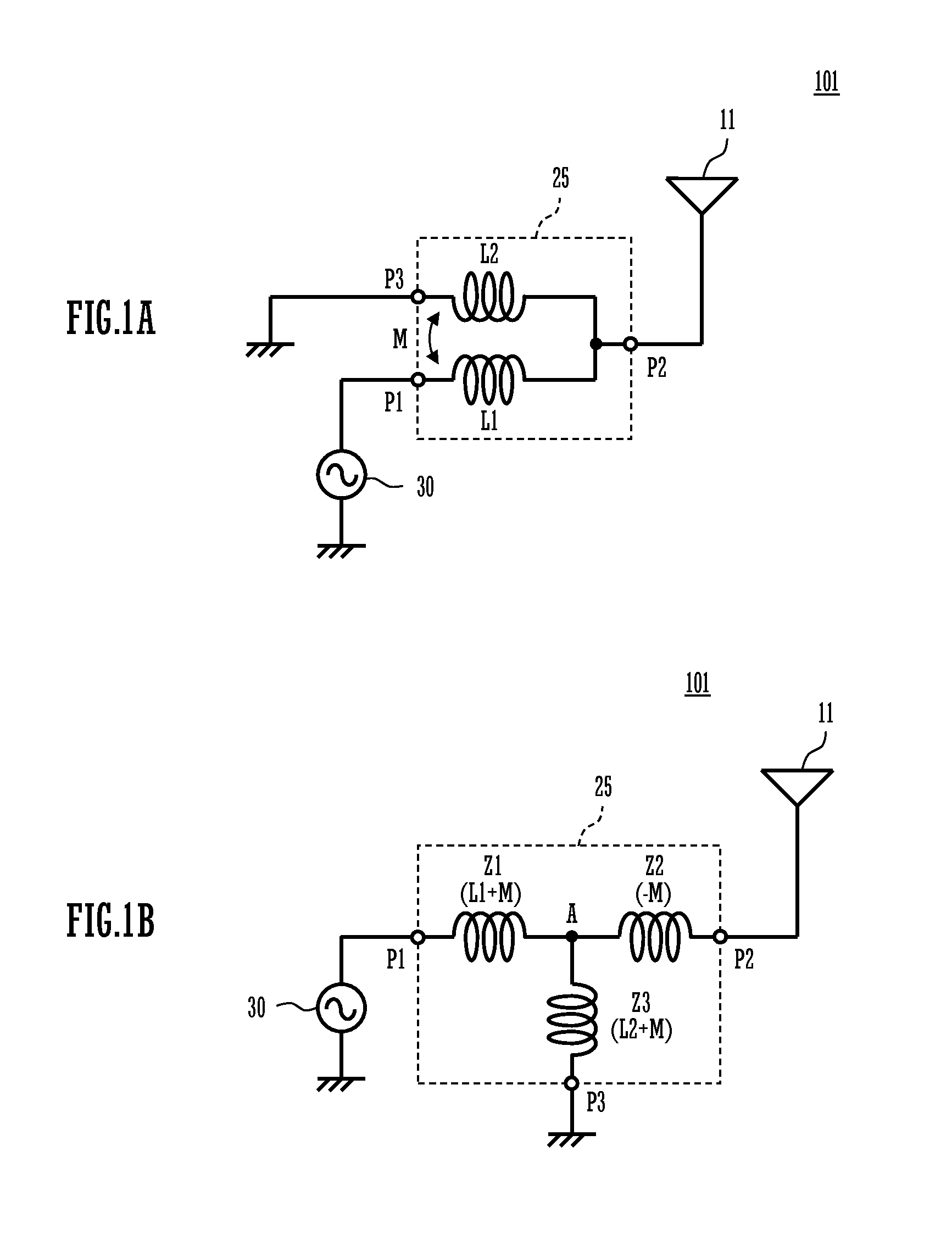
[0052]FIG. 1A is a circuit diagram of an antenna device 101 preferably including an impedance transformation circuit 25 according to a first preferred embodiment of the present invention, and FIG. 1B is an equivalent circuit diagram thereof. For example, in a case of a penta-band supported cellular phone terminal, the cellular phone terminal supports five bands GSM850 / 900 / 1800 / 1900, and UMTS band 1 (GSM is a registered trademark).

[0053]As illustrated in FIG. 1A, the antenna device 101 includes an antenna element 11 and the impedance transformation circuit 25 connected to the antenna element 11. In the Low Band, the antenna element 11 resonates in a fundamental wave mode, and in the High Band, the antenna element 11 resonates in a higher harmonic wave mode. The impedance transformation circuit 25 is connected to a feeder terminal of the antenna element 11. In the impedance transformation circuit 25, a primary coil L1 is inserted between the antenna element 11 and a feeder circuit 30....

second preferred embodiment

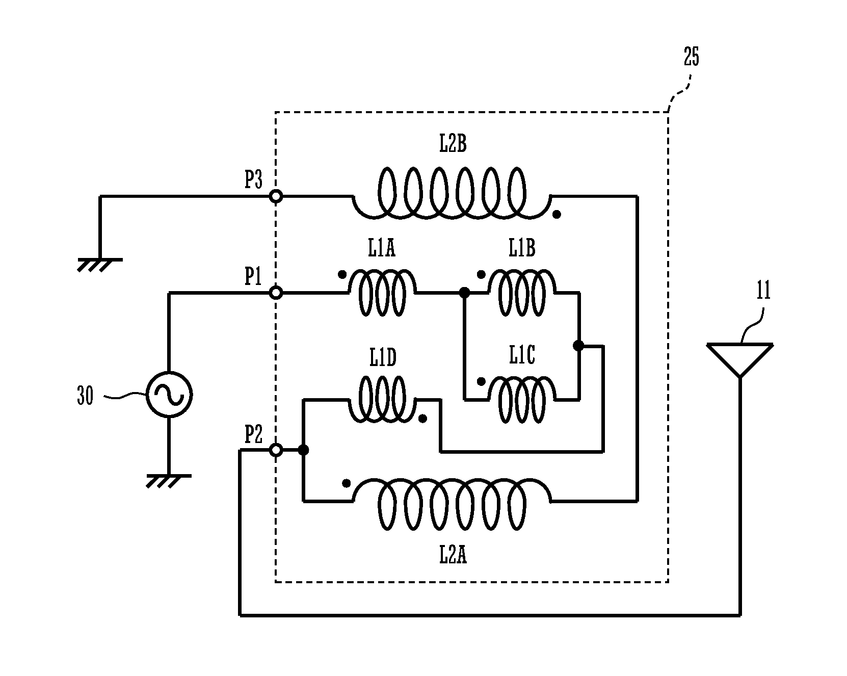
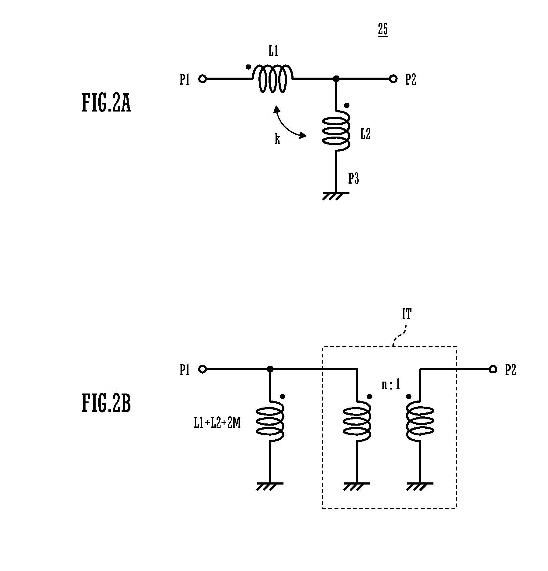
[0079]FIG. 13 is a circuit diagram of an impedance transformation circuit 26 according to a second preferred embodiment of the present invention shown in view of an arrangement relationship between a primary coil and a secondary coil. Like the impedance transformation circuit 25 according to the first preferred embodiment of the present invention, the impedance transformation circuit 26 according to this preferred embodiment preferably includes a stacked body structure in which a dielectric base material layer and a conductive pattern are stacked. The same applies to each of preferred embodiments described after this preferred embodiment. FIG. 14 is a perspective view of various kinds of conductive patterns in the impedance transformation circuit 26. However, the dielectric base material layers on which these conductive patterns are provided are omitted and are not drawn therein.

[0080]As shown in FIG. 14, a first loop-shaped conductor LP1 with conductive patterns L1A, L1B, a second ...

third preferred embodiment

[0084]FIG. 15 is a circuit diagram of an impedance transformation circuit 27A according to a third preferred embodiment of the present invention. FIG. 16 is a figure illustrating a conductive pattern provided in each base material layer of the impedance transformation circuit 27A according to the third preferred embodiment. It is to be noted that the basic configuration is the same as that of the impedance transformation circuit 25 according to the first preferred embodiment, and therefore, the description thereof is omitted here. In this example, a primary coil includes conductive patterns L1B, L1C, and a secondary coil includes conductive patterns L2A, L2B. The conductive pattern L1B, L1C included in the primary coil are adjacent to each other in a stacking direction, and are connected in parallel. The conductive patterns L2A, L2B included in the secondary coil are arranged so as to sandwich the conductive patterns L1B, L1C in the stacking direction, and are connected in series.

[0...


PUM


Abstract

A first coil element includes a first loop-shaped conductor and a second loop-shaped conductor. A second coil element includes a third loop-shaped conductor and a fourth loop-shaped conductor. The first loop-shaped conductor and the second loop-shaped conductor are sandwiched in a stacking direction between the third loop-shaped conductor and the fourth loop-shaped conductor. A conductive pattern which is a portion of the first loop-shaped conductor and a conductive pattern which is a portion of the second loop-shaped conductor are connected in parallel. Then, each of a conductive pattern which is a remaining portion of the first loop-shaped conductor and a conductive pattern which is a remaining portion of the second loop-shaped conductor is connected in series with the parallel circuit.

Description

BACKGROUND OF THE INVENTION[0001]1. Field of the Invention[0002]The present invention relates to an impedance transformation circuit and a wireless communication apparatus preferably for use in an antenna device or other suitable device.[0003]2. Description of the Related Art[0004]Frequency bands used in cellular phones in recent years are very broad bands, and for example, a penta-band-supported cellular terminal is required to support both of a Low Band (for example, 824 MHz to 960 MHz) and a High Band (for example, 1710 MHz to 2170 MHz). For this reason, in order to allow a single antenna to support both of the Low Band and the High Band, the antenna is assigned with different operation modes according to frequency ranges. In normal circumstances, the antenna is designed to support the Low Band in a fundamental wave mode, and is designed to support the High Band in a higher harmonic wave mode. Then, the input impedance of the antenna is different according to the modes (resonance...

Claims


Application Information

Patent Timeline
IPC IPC(8): H03H7/38H01F27/28
CPCH03H7/38H01F2027/2809H01F27/2804H01F19/04H01F38/14H01Q5/50H03H7/0138H03H2001/0085
Inventor ISHIZUKA, KENICHI
Owner MURATA MFG CO LTD
Why Eureka
Try Eureka