
Touch sensor mechanism and manufacturing method thereof

Inactive Publication Date: 2015-07-09
TERA XTAL TECH CORP
View PDF4 Cites 10 Cited by
  • Summary
  • Abstract
  • Description
  • Claims
  • Application Information

AI Technical Summary

Benefits of technology

The present invention provides a touch sensor mechanism and manufacturing method for a touch display device. The mechanism uses a transparent material with high dielectric constant and mechanic strength as a cover lens to reduce thickness. This higher dielectric constant and finger's touching capacitance can adjust the signal-to-noise ratio to a suitable value and prevent sensitivity too high or too low, as well as addressing the issue of sensitivity. Additionally, the mechanism's tolerance to noise caused by crosstalk between sensors and serious electromagnetic interactions due to the large-sized touch panel can be improved, providing more tolerance in circuit design. The sensor device module has at least two sensor devices with lower thickness, higher dielectric constant of the cover lens, longer distance between sensor devices, and lower current of driving circuit to prevent interaction from electromagnetic affect.

Problems solved by technology

In the other words, the touch signal sensing is difficult or distorted due to the thick glass and it will result the judgment mistakes of the touch electronic devices / products.
Therefore, reducing the thickness of cover lens is necessary, however, reducing the thickness of cover lens also reduce the mechanic strength of the touch electronic devices / products.
However, this touch sensor technology is not perfect, for example, the capacitance of this touch sensor technology is easily influenced by the electromagnetic field effect of circuit so at to the effective size of touch panel used this technology is limited to a mid-small size which is equal to or smaller than 17 inches.
Moreover, the larger size and the higher density of sensor will cause the much serious influence by the electromagnetic effect.

Method used


Image

  • Touch sensor mechanism and manufacturing method thereof
  • Touch sensor mechanism and manufacturing method thereof
  • Touch sensor mechanism and manufacturing method thereof

Examples


Embodiment Construction

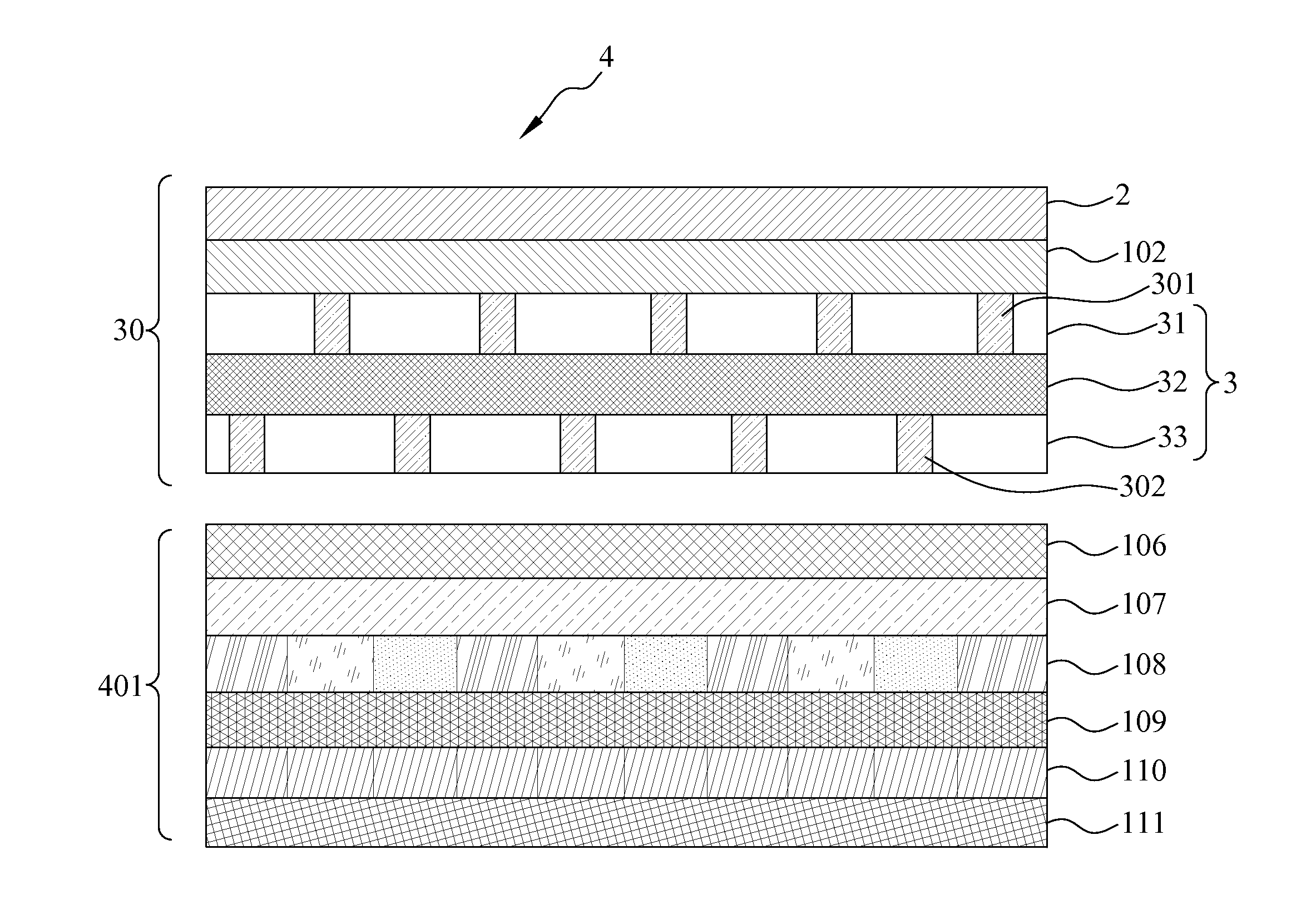
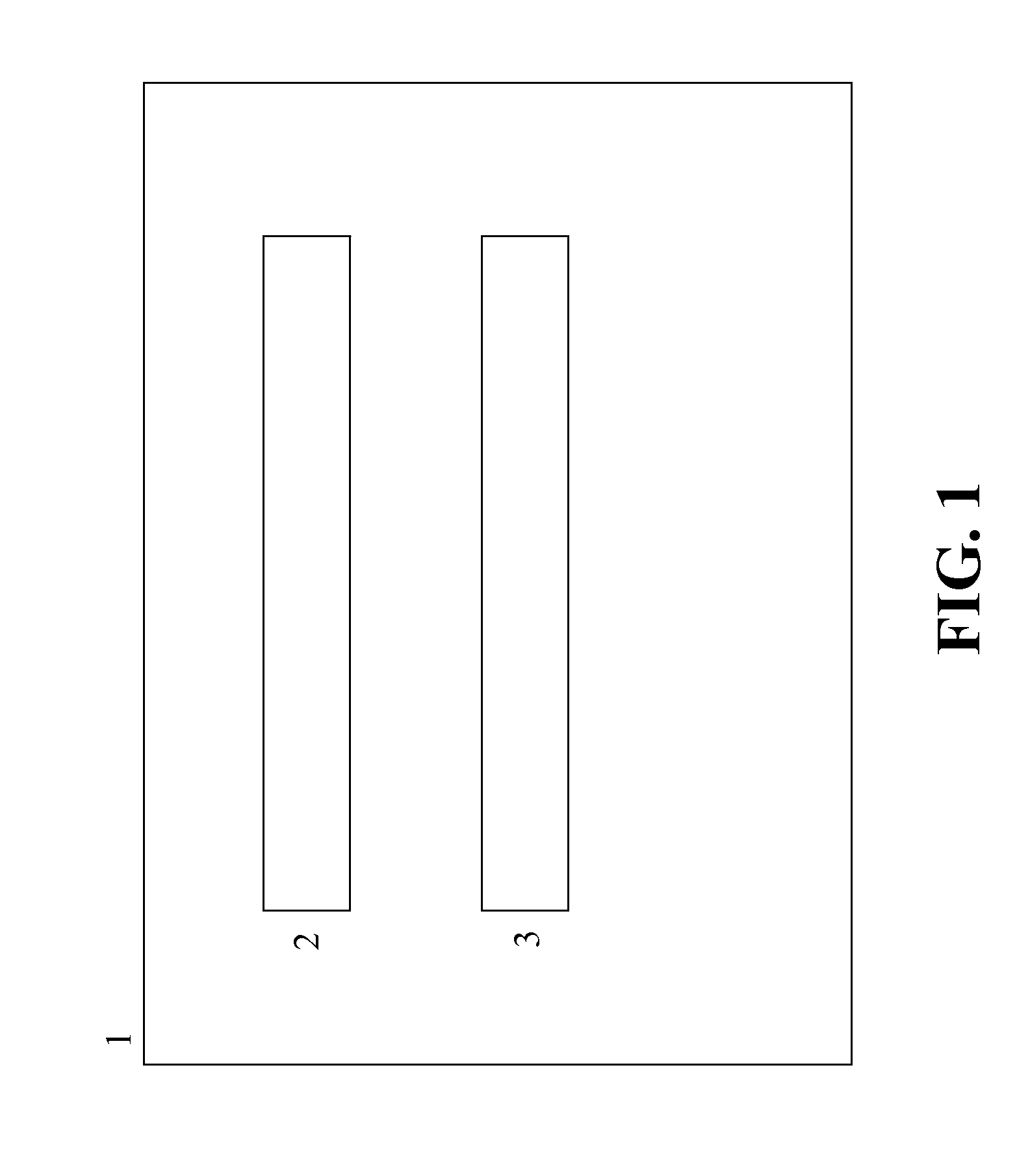
[0046]FIG. 1 is a schematic drawing for illustrating the structure and operation of the touch sensor mechanism of the present invention. As shown in FIG. 1, the touch sensor mechanism 1 of the present invention includes a cover lens 2 and a sensor device module 3. Herein, the touch sensor mechanism 1 can be applied in a touch display device, such as an out-cell LCD touch display device, in-cell LCD touch display device, on-cell LCD touch display device, in-cell / on-cell hybrid LCD touch display device, out-cell OLED touch display device, on-cell OLED touch display device, in-cell OLED touch display device, capacitive fingerprint recognition, capacitive palm print recognition, and handwriting trackpad depending on the real application request.

[0047]Regarding the cover lens 2, the cover lens 2 is a transparent material with a reduced thickness, a high dielectric constant (>4.5) and a high mechanic strength (>700 MPa) for touch. The finger's touching capacitance (CF) can be greatly impr...


PUM

PropertyMeasurementUnit
Pressureaaaaaaaaaa
Thicknessaaaaaaaaaa
Compositionaaaaaaaaaa

Abstract

A touch sensor mechanism for a touch display device, includes a cover lens made by a transparent material having a dielectric constant greater than 4.5 and a compression strength greater than 700 MPa for generating a finger's touching capacitance (CF) while a user's finger of a user touch thereon; and a sensor device module including a plurality of sensor devices having a sensor parasitic capacitance (CP). The cover lens and the sensor device module are disposed in the touch display device in such a manner that a ratio of a standard deviation value (σU) of the finger's touching capacitance (CF) of the cover lens to the sensor parasitic capacitance (CP) of the sensor device module is a signal-to-noise ratio (SNR). The SNR is adjusted along with the finger's touching capacitance (CF) by reducing the thickness of the cover lens.

Description

CROSS-REFERENCES TO RELATED APPLICATIONS[0001]This is a continuation-in-part of U.S. application Ser. No. 13 / 794,655, filed on Mar. 11, 2013, which is incorporated herewith by reference.BACKGROUND OF THE INVENTION[0002]1. Field of the Invention[0003]The present invention generally relates to a touch sensor mechanism and the manufacturing method thereof, more specifically to a touch sensor mechanism and the manufacturing method thereof applied in a touch display device, in which, a transparent material with higher dielectric constant and mechanic strength is implemented as a cover lens for touching thereon. The thickness of the cover lens can be reduced in order to enhance the signal-to-noise ratio (SNR).[0004]2. The Prior Arts[0005]Well-known technology of capacitive touch device using touch sensors already applied in touch electronic devices / products for years. In general, a solution in transitional capacitive touch sensors is using a cover lens with thickness less than 3 mm. In th...

Claims


Application Information

Patent Timeline
IPC IPC(8): G06F3/044G06F3/041
CPCG06F3/044G06F2203/04103G06F3/0416G06F3/0412G02F1/13338G06F2203/04111G06F3/0445G02F1/133331Y10T29/49002
Inventor CHUNG, JUN-WEN
Owner TERA XTAL TECH CORP
Learn More