Tunable soi laser

a laser and silicon technology, applied in semiconductor lasers, laser details, laser optical resonator construction, etc., can solve the problems of low power efficiency, low power efficiency of laser, and low manufacturing cost, so as to reduce the loss, reduce the power efficiency of laser, and reduce the distance

Active Publication Date: 2015-07-23
ROCKLEY PHOTONICS LTD +1
View PDF6 Cites 30 Cited by
  • Summary
  • Abstract
  • Description
  • Claims
  • Application Information

AI Technical Summary

Benefits of technology

[0008]In this way, there is only one gain medium-SOI waveguide interface (i.e. that located at the front end of the gain medium). As a result, the tunable laser of the present invention has an improved power efficiency because the optical losses associated with coupling between the semiconductor gain medium and the waveguide platform are significantly reduced. In addition, the manufacturing complexity is reduced as it is only necessary to align the front end of the gain medium during manufacturing, for example in a flip-chip process.
[0050]In this way, the height (and / or width) of the waveguide is optimized for low loss and mode matching to the gain medium at a first height (and / or width) at the interface to the gain medium but the height (and / or width) is reduced so as to be optimized for speed and power efficiency at a second height (and / or width) at the portion of the waveguide platform where the Distributed Bragg Reflectors are located.

Problems solved by technology

However, they are expensive to manufacture as a result of the need for multiple epitaxial re-growth steps.
To date, demonstrations have been relatively slow to tune so, at present are only suitable for applications in which the speed of tuning is not a key factor.
Of course, the major challenge for SOI photonic integrated platforms is the fact that silicon is not an optical gain medium and does not therefore form an ideal medium for photonic circuits incorporating lasers.
One drawback of such a design is the high optical power loss, particularly due to coupling between the waveguides formed from the silicon substrate and waveguides in any optical devices placed in, grown onto or otherwise incorporated into the platform.

Method used


Image

  • Tunable soi laser
  • Tunable soi laser
  • Tunable soi laser

Examples


first embodiment

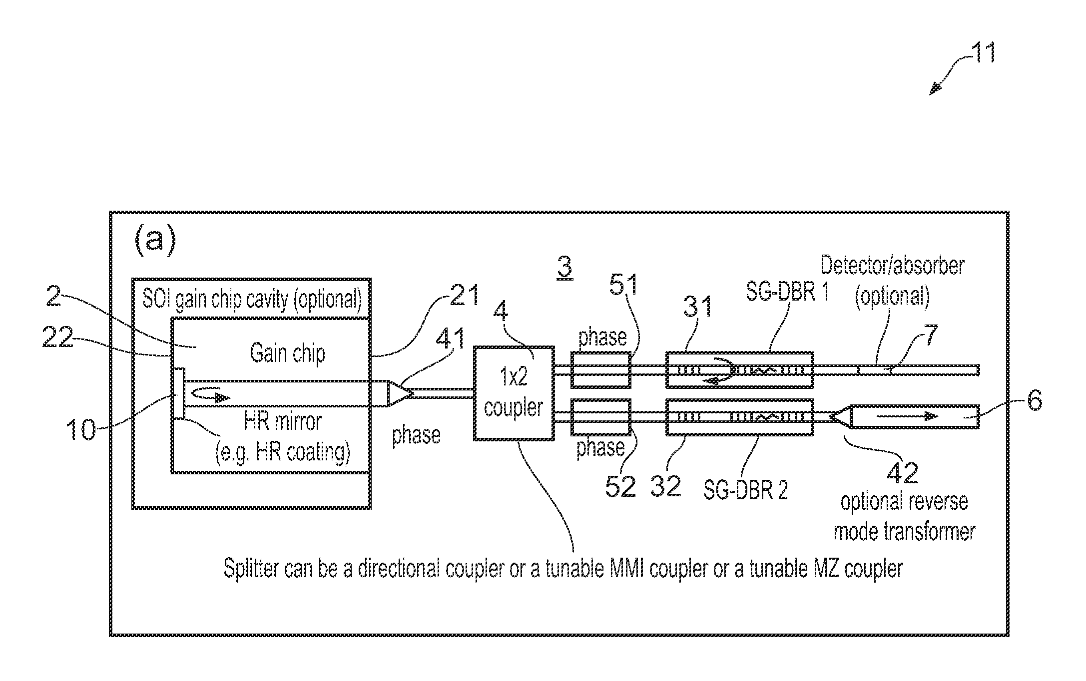
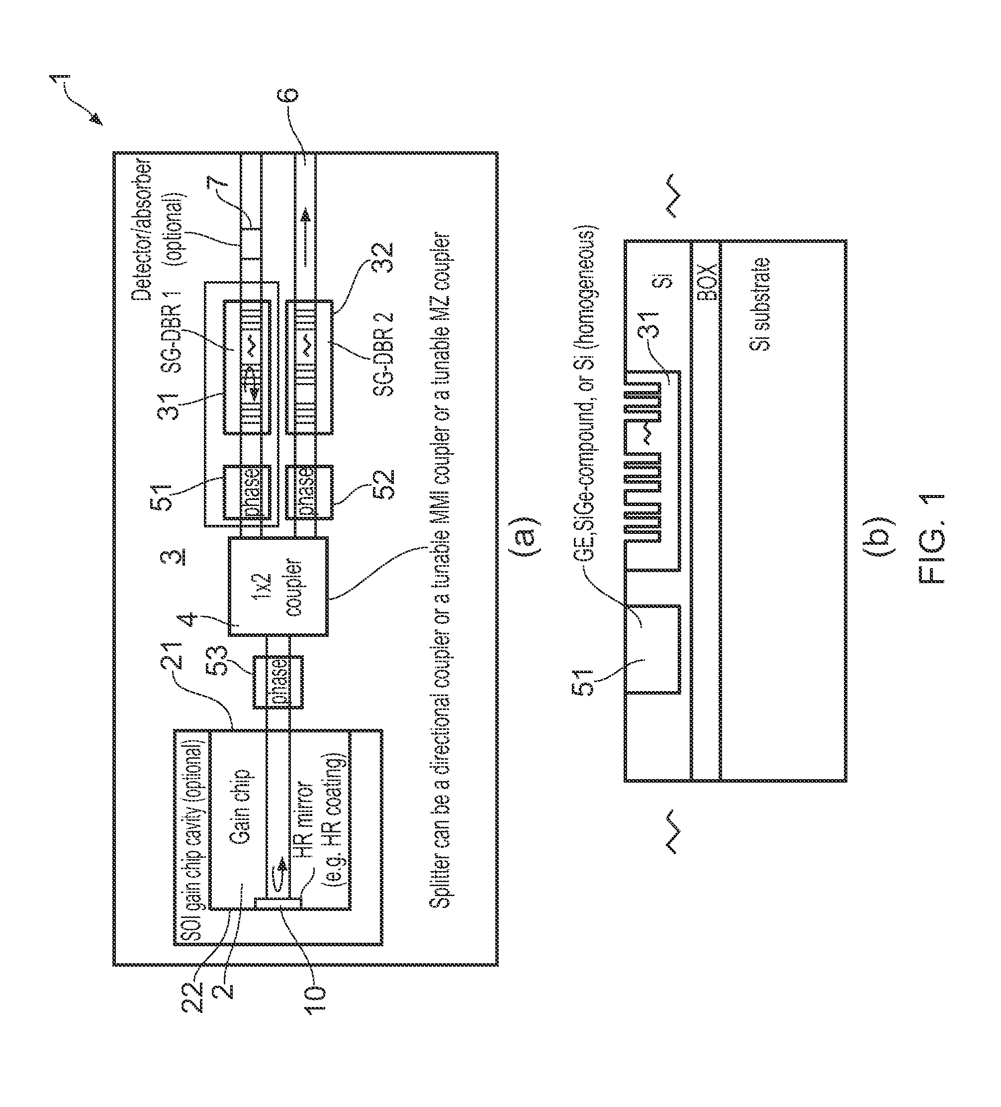
[0067]With reference to FIGS. 1 and 2, a wavelength tunable silicon-on-insulator (SOI) laser, 1, 11, 12, 112 is shown, the laser comprising a laser cavity, made up of a semiconductor gain medium, 2 and a phase-tunable waveguide platform, 3 coupled to the gain medium.

[0068]The semiconductor gain medium has a front end, 21 and a back end, 22 and a mirror of the laser cavity is located at the back end. In the embodiment shown in FIG. 1, the semiconductor gain medium takes the form of a gain chip and the mirror, 10 at the back end of the cavity takes the form of a reflective surface (e.g. a dielectric coating) directly applied to the back end of the gain medium, in this case a reflective back facet of the gain chip. In the embodiment shown in FIG. 1 (a) the waveguide platform includes an SOI gain chip cavity for location of the gain chip.

[0069]The phase-tunable waveguide platform includes a first Distributed Bragg Reflector (DBR), 31 and a second Distributed Bragg Reflector (DBR), 32. I...

third embodiment

[0084]A third embodiment is described with reference to FIGS. 5 to 7, where like reference numerals correspond to those features described above in relation to FIGS. 1 to 4.

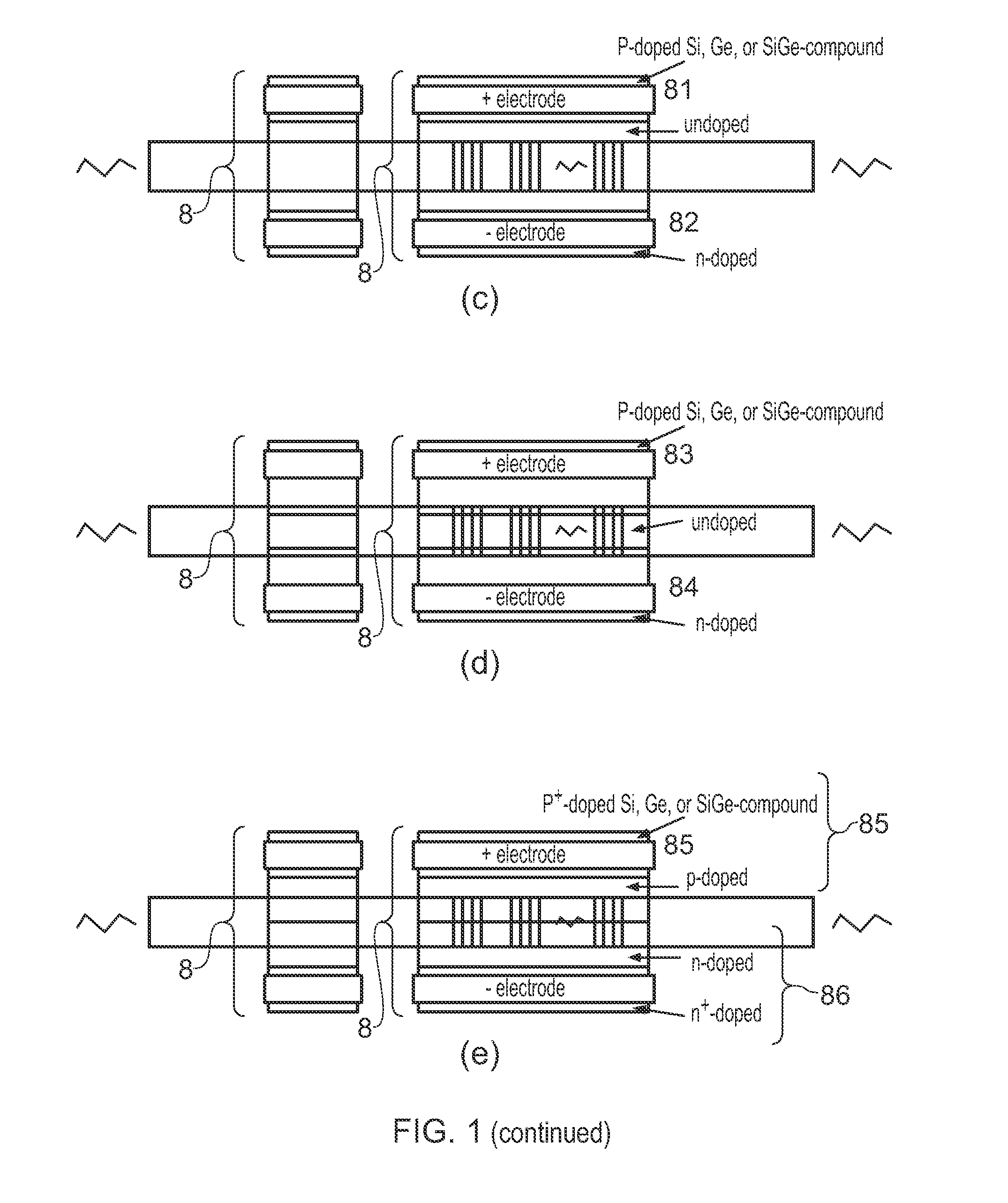
[0085]The third embodiment differs from the first embodiment in that the first Distributed Bragg Reflector is a Sectioned Grating-Distributed Bragg reflector (SG-DBR), 31 and the second Distributed Bragg Reflector is a Digital Supermode-Distributed Bragg Reflector (DS-DBR) 33 operating in transmission. In the embodiment shown in FIG. 5, the two DBRs are arranged in series and each DBR is a phase-tunable DBR so includes a phase tuning region, 8.

[0086]Referring specifically to the DS-DBR of the third embodiment, in FIGS. 5 (c) and (d), the phase tuning region is a p-i-n junction with positive electrodes, 88 located in the p-doped region and negative electrodes, 89 located in the n-doped region. In FIG. 5(c), the phase tuning region of the DS-DBR includes p- and n-doped regions which are detached from waveguide ridg...

second embodiment

[0095]As with the transition region described in relation to the second embodiment, the transition region of this embodiment is a transition from a waveguide of a first height, T1 and first width, w1 to a waveguide of a second height, T2 and a second width w2; the second height being less than the first height and the second width being less than the first width. In this case, the first and second Distributed Bragg Reflectors are located in a waveguide of a second height, T2 and second width w2.

[0096]An optional inverse transition region (or mode transformer) can be used after the SG-DBR mirror (i.e. outside the laser cavity) to expand the mode back to the original waveguide size. Alternatively the smaller waveguide dimensions can continue into the other regions of the SOI chip. This embodiment with reduced waveguide dimensions can produce phase modulators with faster tuning speeds and lower power consumption, at the expense of adding the additional optical loss introduced by the mo...


PUM


Abstract

A wavelength tunable silicon-on-insulator (SOI) laser comprising: a laser cavity including: a semiconductor gain medium having a front end and a back end; and a phase-tunable waveguide platform coupled to the front end of the semiconductor gain medium; wherein the phase-tunable waveguide platform includes a first Distributed Bragg Reflector (DBR) and a second Distributed Bragg Reflector (DBR); at least one of the Distributed Bragg Reflectors having a comb reflectance spectrum; and wherein a mirror of the laser cavity is located at the back end of the semiconductor gain medium.

Description

FIELD OF THE INVENTION[0001]The present invention relates to a wavelength tunable silicon-on-insulator (SOI) laser, particularly to a wavelength tunable SOI laser having a semiconductor gain medium with a front and a back end and a mirror of the laser cavity located at the back end of the semiconductor gain medium.BACKGROUND OF THE INVENTION[0002]Tunable semiconductor lasers are often used for applications in which an occasional but precise tuning of wavelength is required. They provide excellent wavelength stability and are typically manufactured as monolithic photonic integrated circuits in a gain medium such as a III-V semiconductor material. However, they are expensive to manufacture as a result of the need for multiple epitaxial re-growth steps. To date, demonstrations have been relatively slow to tune so, at present are only suitable for applications in which the speed of tuning is not a key factor.[0003]Particularly in applications where the precise wavelength of the laser is...

Claims


Application Information

Patent Timeline
Patent Type & Authority Applications(United States)
IPC IPC(8): H01S5/125H01S5/32H01S5/30H01S5/34H01S5/10H01S5/02
CPCH01S5/125H01S5/1007H01S5/3224H01S5/3031H01S5/3427H01S5/021H01S3/1055H01S3/106H01S5/028H01S5/1209H01S5/142G02B6/26G02B6/42H01S3/0637H01S5/0625H01S5/141
Inventor RICKMAN, ANDREWZILKIE, AARON JOHN
Owner ROCKLEY PHOTONICS LTD
Why Eureka
Try Eureka