Small-Grain Three-Dimensional Memory

Active Publication Date: 2015-07-30
HANGZHOU HAICUN INFORMATION TECH +1
View PDF0 Cites 19 Cited by
  • Summary
  • Abstract
  • Description
  • Claims
  • Application Information

AI Technical Summary

Benefits of technology

The present invention is about a new type of diode for use in 3D-M. This diode is made up of small grains of material, which helps to reduce performance variations and improve the consistency of the diode's behavior. By using small-grain materials, the diode can achieve tight current control and enable multi-bit-per-cell for the 3D-M. Compared to traditional single-crystalline transistors, the scaling of small-grain diodes is simpler, which makes it easier to produce smaller memory cells. This also means that the critical dimension of the memory level can be smaller than the critical dimension of the substrate level, which is currently achievable with flash memory.

Problems solved by technology

This leads to unacceptable read / write error rate.
Furthermore, a large current fluctuation becomes more troublesome when multi-bit-per-cell is employed to increase the storage density of a 3D-Msp, because multi-bit-per-cell requires a tight current control.
In sum, the prior-art 3D-MSP has a poor performance and a limited storage density.

Method used


Image

  • Small-Grain Three-Dimensional Memory
  • Small-Grain Three-Dimensional Memory
  • Small-Grain Three-Dimensional Memory

Examples


Embodiment Construction

[0022]Those of ordinary skills in the art will realize that the following description of the present invention is illustrative only and is not intended to be in any way limiting. Other embodiments of the invention will readily suggest themselves to such skilled persons from an examination of the within disclosure.

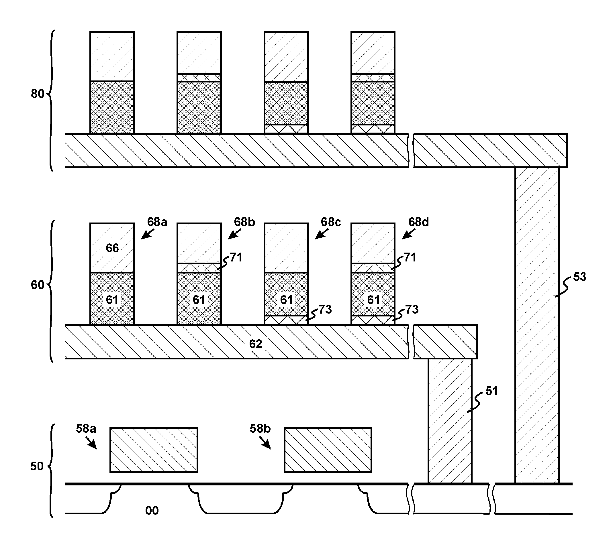
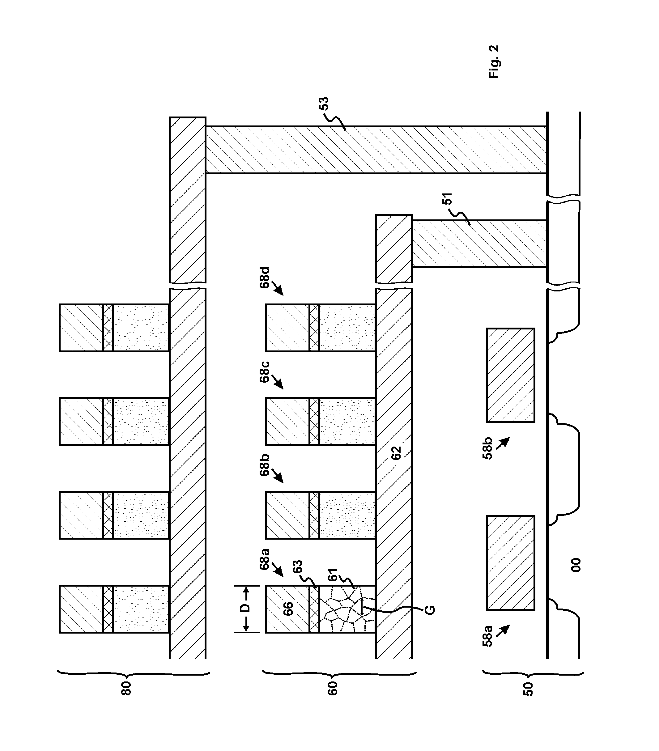
[0023]Referring now to FIG. 2, a preferred small-grain 3D-M (3D-MSG) is disclosed. It comprises a substrate level 50 and at least two memory levels 60, 80. The substrate level 50 comprises a plurality of functional transistors 58a, 58b. Formed in the substrate 00, these transistors are single-crystalline transistors. Here, “functional transistors”, unlike “dummy transistors”, perform certain chip functions. These functional transistors could form a peripheral circuit for the 3D-M, a processing circuit which processes the 3D-M data, and / or a memory circuit (e.g. a transistor-based memory, such as a RAM array or a ROM array) which functions as a buffer or redundancy for the 3...


PUM


Abstract

The present invention discloses a small-grain three-dimensional memory (3D-MSG). Each of its memory cells comprises a thin-film diode with critical dimension no larger than 40 nm. The thin-film diode comprises at least a small-grain material, whose grain size G is substantially smaller than the diode size D. The small-grain material is preferably a nano-crystalline material or an amorphous material. The critical dimension f of the small-grain diode is smaller than the critical dimension F of the single-crystalline transistor.

Description

CROSS-REFERENCE TO RELATED APPLICATIONS[0001]This application is a continuation-in-part of “Small-Grain Three-Dimensional Memory”, application Ser. No. 13 / 848,018, filed Mar. 20, 2013, which claims foreign priority of a Chinese Patent Application Ser. No. 201210089545.5, “Small-Grain Three-Dimensional Memory”, filed in People's Republic of China on Mar. 30, 2012.BACKGROUND[0002]1. Technical Field of the Invention[0003]The present invention relates to the field of integrated circuit, and more particularly to diode-based monolithic three-dimensional semiconductor memory.[0004]2. Prior Arts[0005]Three-dimensional memory (3D-M) is a monolithic semiconductor memory. It comprises a plurality of vertically stacked memory levels. As illustrated in FIG. 1, a 3D-M comprises at least a substrate level 30 and a memory level 40. The substrate level 30 comprises a plurality of transistors (38a . . . ). Formed in a single-crystalline semiconductor substrate 00, these transistors are single-crystal...

Claims


Application Information

Patent Timeline
IPC IPC(8): H01L27/24H01L27/112
CPCH01L27/2481H01L27/11213H01L27/2436H01L27/11206G11C5/02G11C11/5692G11C13/0004G11C13/0007G11C13/0011G11C17/10G11C17/16G11C2213/71G11C2213/73H01L27/1021H10B63/84H10B63/30H10N70/245H10N70/231H10N70/20H10N70/882H10N70/8833
Inventor ZHANG, GUOBIAOYU, BINYU, HONGYUHE, JINKANG, JINFENGLIU, ZHIWEI
Owner HANGZHOU HAICUN INFORMATION TECH
Why Eureka
Try Eureka