Lead-Free Solder Ball

a solder ball and lead-free technology, applied in the direction of soldering apparatus, manufacturing tools, capacitors, etc., can solve the problems of inferior resistance to drop impacts, inability to supply solder from the exterior to the electrode located at the center of the substrate, and inability to supply solder to the electrode, so as to reduce the amount of ni compounds, prevent fusion defects, and reduce the effect of resistance to drop impacts

Active Publication Date: 2015-08-06
SENJU METAL IND CO LTD
View PDF2 Cites 8 Cited by
  • Summary
  • Abstract
  • Description
  • Claims
  • Application Information

AI Technical Summary

Benefits of technology

[0027]In order to decrease the amount of Ni compounds which precipitate on the surface of a solder ball made of a solder alloy having a Sn—Ag—Cu—Ni composition, the present inventors focused on the fact that intermetallic compounds of Sn, Cu, and Ni do not precipitate on a solder ball surface if the content of Cu which reacts with Ni is decreased. However, if the Cu content is decreased, resistance to drop impacts decreases when soldering to Cu electrodes is carried out. The present inventors found that by setting the content of Cu which is added to a solder alloy in the vicinity of 0.75 mass % which is near the eutectic point, consumption of Cu due to network formation and consumption of Cu due to the formation of compounds of Cu and Ni are balanced, and compounds of Cu and Ni no longe

Problems solved by technology

However, supplying solder to each electrode and carrying out soldering requires a great deal of effort, and solder cannot be supplied from the exterior to electrodes located at the center of a substrate.
These lead-free solder alloys have excellent resistance to thermal fatigue, but when portable electronic equipment using solder balls having these solder alloy compositions is dropped, interfacial peeling in which peeling takes place from the bonding interface of the solder balls easily occurs, so resistance to drop impacts is inferior.
However, these Sn—Ag—Cu or Sn—Ag—Cu—Ni based solder compositions used in solder balls have poor wettability compared to conventional Sn—Pb based solders, and when BGAs are moun

Method used


Image

  • Lead-Free Solder Ball
  • Lead-Free Solder Ball
  • Lead-Free Solder Ball

Examples


examples

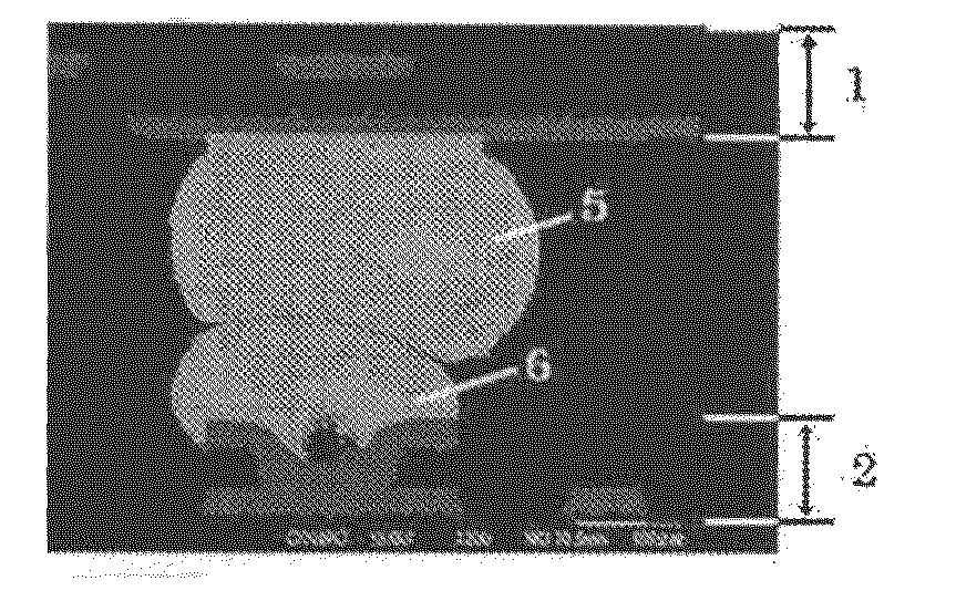
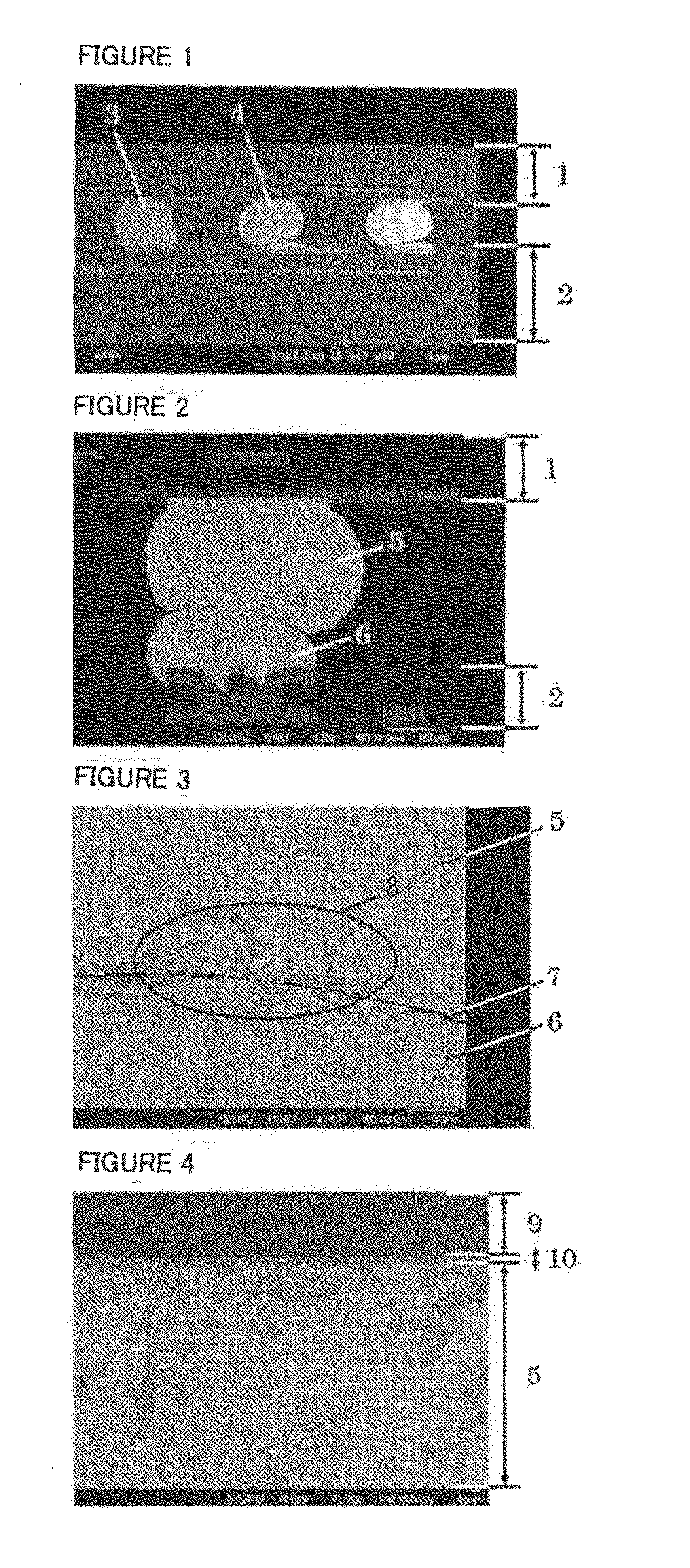
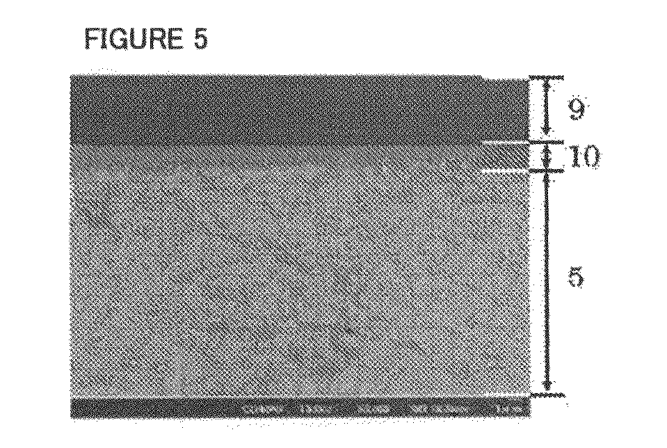
[0047]Solder alloys having the compositions shown in Table 1 were prepared, and they were formed into solder balls having a diameter of 0.3 mm by the gas atomization method. The resulting solder balls were used to evaluate with respect to fusion defects and by a thermal fatigue test and a drop impact test.

TABLE 1NumberNumber ofNumber ofSolder composition (mass %)of fusioncycles in ther-drops in dropSnAgCuNiFeCoPtBiInSbPGedefectsmal fatigue testimpact testRemarksExam-1Rem1.60.750.0701623141ples2Rem2.00.750.07019001183Rem2.50.750.0701971914Rem2.90.750.0702373665Rem1.80.700.05016961336Rem2.90.800.0802296577Rem2.50.700.0802008888Rem2.50.800.0502181829Rem2.00.750.070.010191513510Rem2.00.750.070.0080193512811Rem2.00.750.070.050190313312Rem2.00.750.070.10194211513Rem2.00.750.070.10192811214Rem2.00.750.070.070193012015Rem2.00.750.070.0030189511716Rem2.00.750.070.00801890116Com-1Rem3.00.50024641para-2Rem1.00.50108981tive3Rem1.00.750.0715977156exam-4Rem3.50.750.070248918ples5Rem2.50.600.07019...


PUM

PropertyMeasurementUnit
Percent by massaaaaaaaaaa

Abstract

A lead-free solder ball is provided which suppresses interfacial peeling in a bonding interface of a solder ball, fusion defects which develop between the solder ball and solder paste, and which can be used both with Ni electrodes plated with Au or the like and Cu electrodes having a water-soluble preflux applied atop Cu. The lead-free solder ball for electrodes of BGAs or CSPs consists of 1.6-2.9 mass % of Ag, 0.7-0.8 mass % of Cu, 0.05-0.08 mass % of Ni, and a remainder of Sn. It has excellent resistance to thermal fatigue and to drop impacts regardless of the type of electrodes of a printed circuit board to which it is bonded, which are Cu electrodes or Ni electrodes having Au plating or Au/Pd plating as surface treatment. The composition may include at least one element selected from Fe, Co, and Pt in a total amount of 0.003-0.1 mass % or at least one element selected from Bi, In, Sb, P, and Ge in a total emount of 0.003-0.1 mass %.

Description

TECHNICAL FIELD[0001]This invention relates to a lead-free solder ball used for electrodes of electronic parts such as semiconductors.[0002]In particular, it relates to a lead-free solder ball which has few problems due to fusion defects.BACKGROUND ART[0003]Recently, due to decreases in the size of electronic equipment and increases in the speed of electrical signals, electronic parts used in electronic equipment are becoming smaller in size and multifunctional. Examples of electronic parts which have become smaller in size and multifunctional are BGAs (ball grid arrays), CSPs (chip size packages), and MCMs (multichip modules) (collectively referred to below as BGAs). BGAs have electrodes disposed in a lattice-like pattern on the rear surface of a BGA substrate.[0004]In order to mount a BGA on a printed circuit board, electrodes of the BGA and lands of the printed circuit board are connected with each other by solder. However, supplying solder to each electrode and carrying out sold...

Claims


Application Information

Patent Timeline
IPC IPC(8): H01L23/00C22C13/00H05K3/34B23K35/02B23K1/00H01B1/02B23K35/26
CPCB23K35/26H01L2924/01322C22C13/02B23K35/0261H01L24/13H05K3/3457H05K2203/041H01L2924/15311H01L2924/2076H01L2924/01083H01L2924/01078H01L2924/01051H01L2924/0105H01L2924/01049H01L2924/01047H01L2924/01032H01L2924/01028H01L2924/01027H01L2924/01026H01L2924/01015H01L2224/13147H01L2224/1301H01L24/11H01B1/02B23K35/262B23K35/0222B23K1/0016H01L2924/181H01L2924/15331H01L2924/15321H01L2924/014C22C13/00H01L2924/00H05K3/34H05K3/3463H01L24/05H01L2224/0401H01L2224/05073H01L2224/05082H01L2224/05155H01L2224/05164H01L2224/05644H01L2224/05647H01L2224/13111H01L2924/01029H01L2924/00014
Inventor YAMANAKA, YOSHIETACHIBANA, KENYOSHIKAWA, SHUNSAKUNOMURA, HIKARU
Owner SENJU METAL IND CO LTD
Why Eureka
Try Eureka