

Pixel electrode, display device, method of manufacturing pixel electrode
a technology of pixel electrode and display device, which is applied in the direction of semiconductor/solid-state device details, instruments, semiconductor devices, etc., can solve the problems of easy corrosion of film, low durability and reliability, etc., and achieve the effect of significant reducing the reflectivity of the pixel electrode 44b
- Summary
- Abstract
- Description
- Claims
- Application Information
AI Technical Summary
Benefits of technology
Problems solved by technology
Method used
Image

Examples
first embodiment
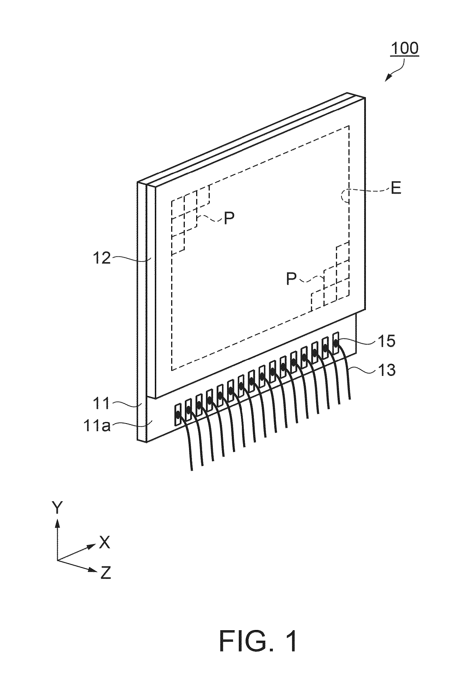
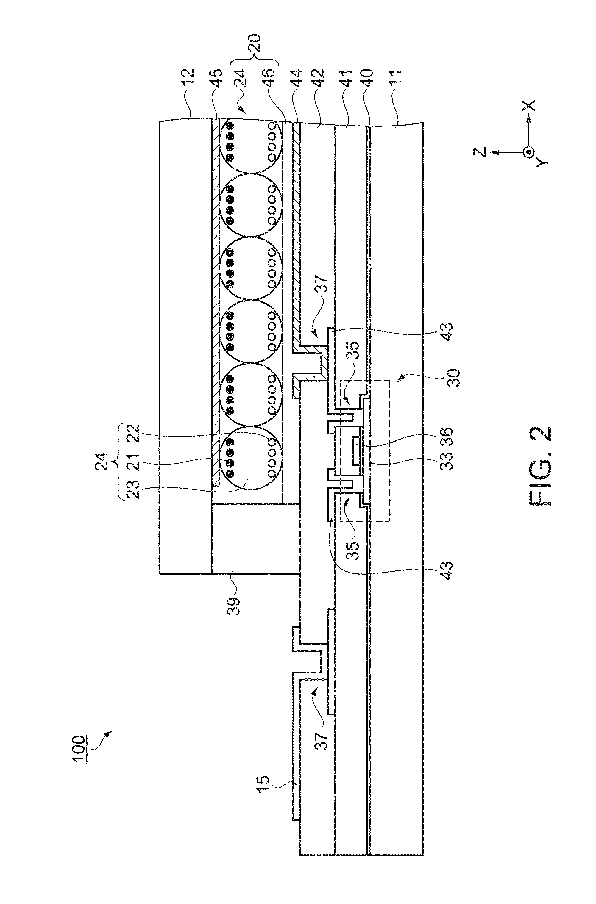
[0039]First, prior to the explanation of a pixel electrode according to the embodiment, a display device using the pixel electrode will be explained using FIGS. 1 and 2 by taking an electrophoretic display device as an example. FIG. 1 is a schematic perspective view showing a configuration of the electrophoretic display device, and FIG. 2 is a schematic sectional view showing structures of pixels etc. in the electrophoretic display device.
Electrophoretic Display Device
[0040]As shown in FIG. 1, the electrophoretic display device 100 as the display device of the embodiment has a device substrate 11 and an opposed substrate 12 provided to face each other. Further, an electrophoretic layer 20 (see FIG. 2) as a display layer is provided between the pair of substrates. Note that, in the embodiment, both of the pair of substrates are rectangular, but not limited to the shape.
[0041]The electrophoretic layer 20 has a plurality of regions sectioned in a matrix form between the pair of substra...
embodiment
Advantages of Embodiment
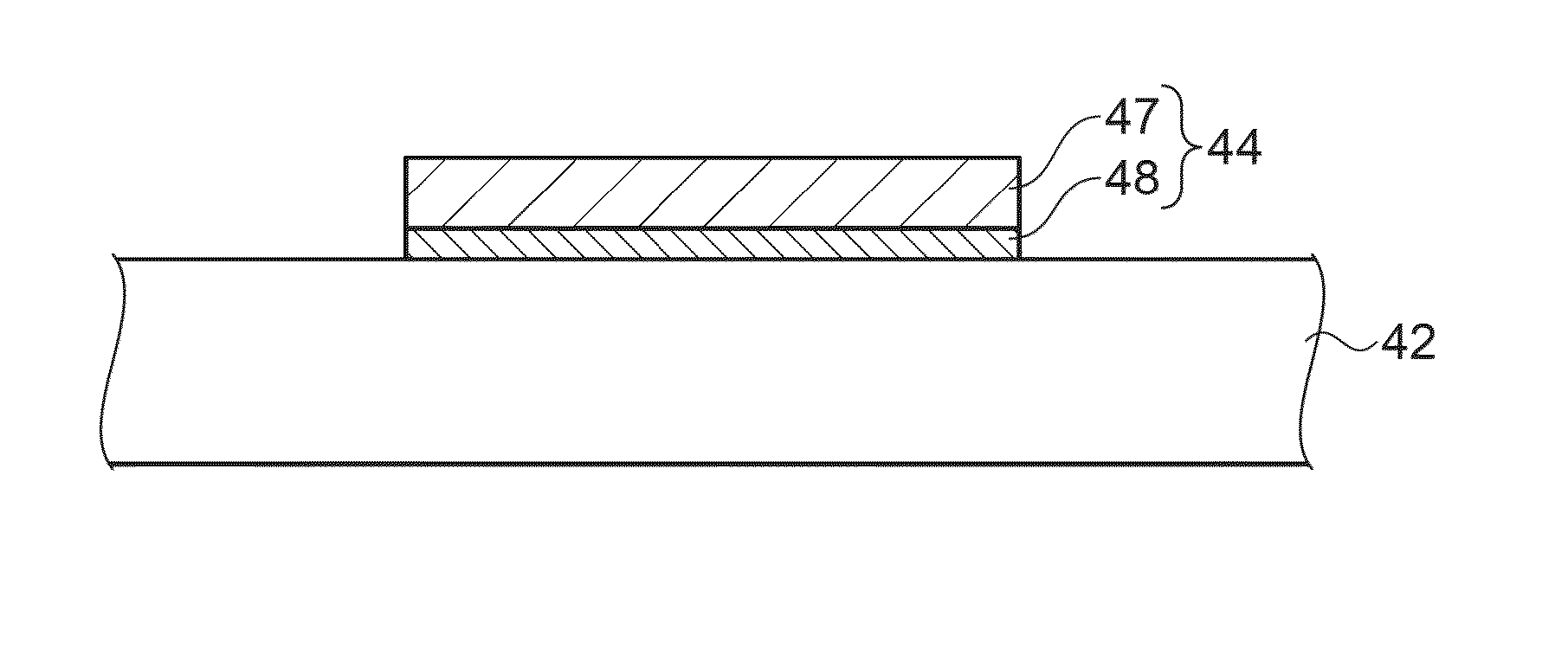
[0077]FIGS. 4 to 6B show advantages by the pixel electrode of the embodiment. FIG. 4 shows a result of a plan view (of a pixel electrode 44a) after rectangular wave having an amplitude of 0 V to 10 V (volts) is applied to the pixel electrode 44a with a smaller exposed area of the Ti layer 48 in a predetermined time. FIG. 5 shows a result of a plan view (of a pixel electrode 44b) after rectangular wave having an amplitude of 0 V to 10 V (volts) is applied to the pixel electrode 44a with a larger exposed area of the Ti layer 48 in a predetermined time.
[0078]FIGS. 6A and 6B show sections of the pixel electrodes (44a, 44b) used for the above described experiments. Specifically, FIG. 6A is a sectional view of the pixel electrode 44a having the smaller exposed area of the Ti layer 48 and FIG. 6B is a sectional view of the pixel electrode 44b having the larger exposed area of the Ti layer 48. In FIGS. 6A and 6B, only the second interlayer insulating film 42 is shown...
modified example 1
[0105]The electrophoretic display device 100 of the embodiment is formed using the electrophoretic layer 20 including the microcapsules 24 as shown in FIG. 2. However, the electrophoretic layer 20 is not limited to that including the microcapsules 24. For example, partition walls surrounding the respective pixel electrodes 44 are formed and respective recessed portions formed by the partition walls and the pixel electrodes 44 are filled with the dispersion media 23 containing the black particles 21 and the white particles 22, and thereby, the electrophoretic layer 20 may be formed. In this case, the pixel electrodes 44 are in contact with the dispersion media 23 containing electrolyte, and the advantage of the invention is obtained.
PUM
| Property | Measurement | Unit |
|---|---|---|
| diameters | aaaaa | aaaaa |
| electrode potential | aaaaa | aaaaa |
| electrode potential | aaaaa | aaaaa |
Abstract
Description
Claims
Application Information