METHOD OF ENHANCING HIGH-k FILM NUCLEATION RATE AND ELECTRICAL MOBILITY IN A SEMICONDUCTOR DEVICE BY MICROWAVE PLASMA TREATMENT

a technology of high-k film nucleation rate and electrical mobility, which is applied in the direction of coatings, chemical vapor deposition coatings, electric discharge tubes, etc., can solve problems such as device degradation, and achieve the effects of increasing electrical mobility, reducing the thickness of the interface layer, and increasing electrical mobility

Active Publication Date: 2015-09-03
TOKYO ELECTRON LTD
View PDF9 Cites 6 Cited by
  • Summary
  • Abstract
  • Description
  • Claims
  • Application Information

AI Technical Summary

Benefits of technology

[0006]According to another embodiment, the method includes providing a substrate in a process chamber, flowing a process gas consisting of H2 and optionally a noble gas into the process chamber, and forming plasma excited species from the process gas by a microwave plasma source. The method further includes exposing an interface layer on the substrate to the plasma excited species to form a modified interface layer with increased electrical mobility, where the exposing reduces a thickness of the interface layer, and depositing a high-k film by ALD on the modified interface layer, where the high-k film nucleates at a higher rate on the modified interface layer rate than on the interface layer.
[0007]According to yet another embodiment, the method includes providing a germanium-containing substrate in a process chamber, flowing a process gas consisting of H2 and optionally a noble gas into the process chamber, and forming plasma excited species from the process gas by a microwave plasma source. The method further includes exposing a germanium-containing interface layer on the substrate to the plasma excited species to form a modified germanium-containing interface layer with increased electrical mobility, and depositing a high-k film by ALD on the modified germanium-containing interface layer, where the high-k film nucleates at a higher rate on the modified germanium-containing interface layer rate than on the germanium-containing interface layer.

Problems solved by technology

However, one of the issues with the high mobility channel is the poor oxide and interface quality that can result in device degradation.

Method used


Image

  • METHOD OF ENHANCING HIGH-k FILM NUCLEATION RATE AND ELECTRICAL MOBILITY IN A SEMICONDUCTOR DEVICE BY MICROWAVE PLASMA TREATMENT
  • METHOD OF ENHANCING HIGH-k FILM NUCLEATION RATE AND ELECTRICAL MOBILITY IN A SEMICONDUCTOR DEVICE BY MICROWAVE PLASMA TREATMENT
  • METHOD OF ENHANCING HIGH-k FILM NUCLEATION RATE AND ELECTRICAL MOBILITY IN A SEMICONDUCTOR DEVICE BY MICROWAVE PLASMA TREATMENT

Examples


Embodiment Construction

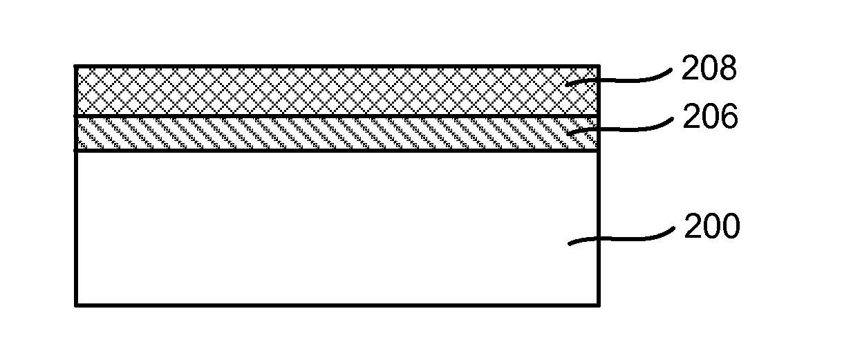
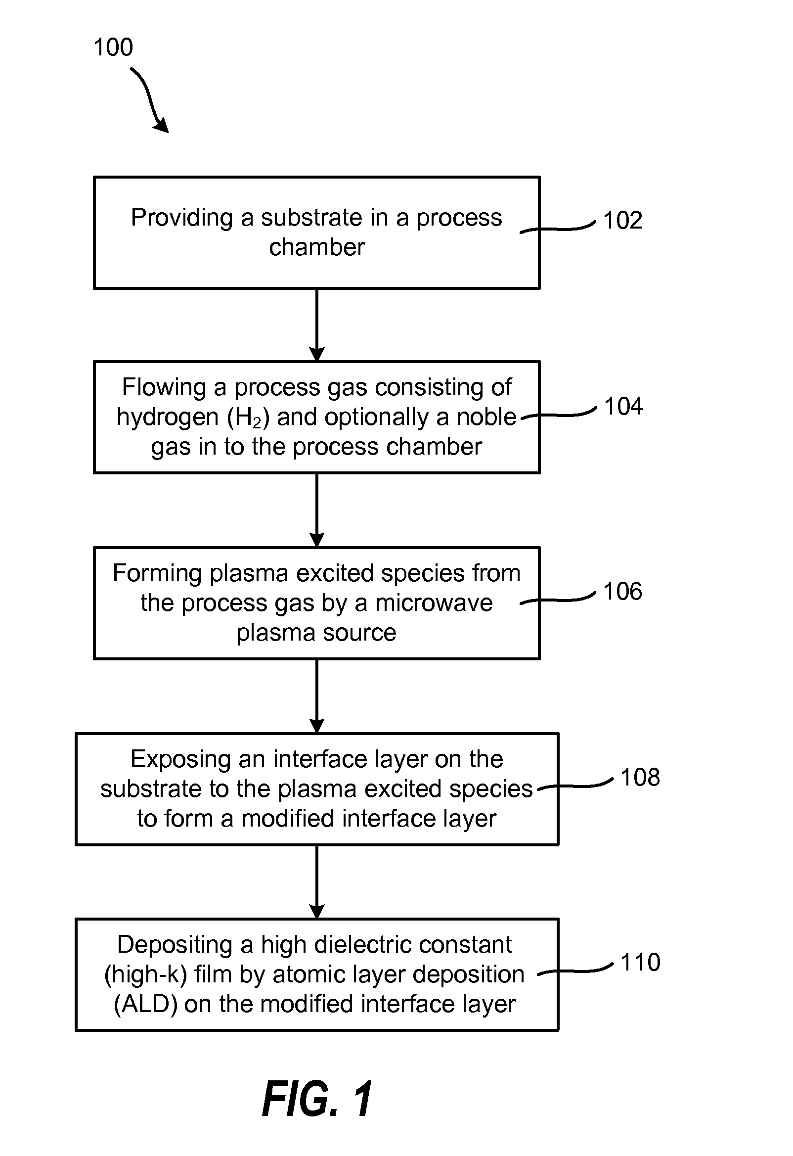
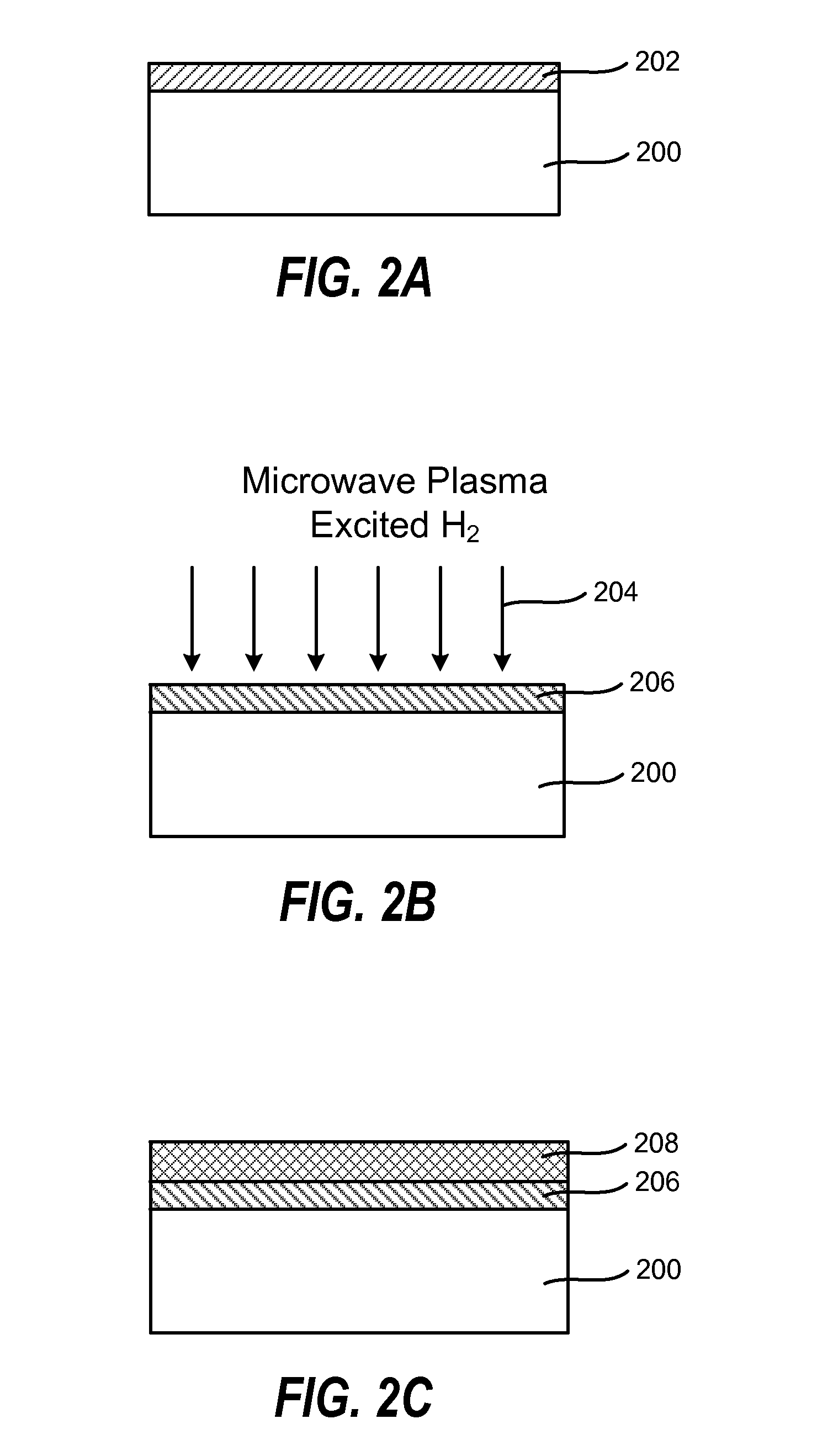
[0020]Embodiments of the invention are described below in reference to the Figures. According to one embodiment, a method is provided for forming a semiconductor device. The method uses microwave plasma treatment to enhance high-k film nucleation rate and electrical mobility in the semiconductor device.

[0021]According to one embodiment, the method includes providing a substrate in a process chamber, flowing a process gas consisting of H2 and optionally a noble gas into the process chamber, and forming plasma excited species from the process gas by a microwave plasma source. The method further includes exposing an interface layer on the substrate to the plasma excited species to form a modified interface layer with increased electrical mobility, and depositing a high-k film on the modified interface layer. The exposure of the interface layer to plasma excited species can reduce the thickness of the interface layer and the modified interface layer has been found to be more reactive th...


PUM

PropertyMeasurementUnit
temperatureaaaaaaaaaa

Abstract

A method for forming a semiconductor device is provided in several embodiments. According to one embodiment, the method includes providing a substrate in a process chamber, flowing a process gas consisting of hydrogen (H2) and optionally a noble gas into the process chamber, forming plasma excited species from the process gas by a microwave plasma source. The method further includes exposing an interface layer on the substrate to the plasma excited species to form a modified interface layer, and depositing a high dielectric constant (high-k) film by atomic layer deposition (ALD) on the modified interface layer. In some embodiments, the modified interface layer has higher electrical mobility than the interface layer, and the high-k film nucleates at a higher rate on the modified interface layer rate than on the interface layer.

Description

CROSS-REFERENCE TO RELATED APPLICATIONS[0001]This application is related to and claims priority to U.S. Provisional application Ser. No. 61 / 946,829 filed on Mar. 2, 2014, the entire contents of which are herein incorporated by reference. This application is related to and claims priority to U.S. Provisional application Ser. No. 61 / 986,995 filed on May 1, 2014, the entire contents of which are herein incorporated by reference.FIELD OF THE INVENTION[0002]The present invention generally relates to a method of enhancing high-dielectric constant (high-k) film nucleation rate and electrical mobility in a semiconductor device by microwave plasma treatment of an interface layer on a substrate prior to deposition of a high-k film on the interface layer.BACKGROUND OF THE INVENTION[0003]Devices with a high-mobility channel, such as Si, SiGe, Ge and compound semiconductors offer the possibility of increased device performance beyond traditional Si-based devices. In particular, Ge and Ge-contain...

Claims


Application Information

Patent Timeline
Patent Type & Authority Applications(United States)
IPC IPC(8): H01L21/02H01L21/3213H01L21/311H01L21/28
CPCH01L21/02315H01L21/28026H01L21/31111H01L21/0228H01L21/32136C23C16/0272C23C16/405C23C16/45525H01J37/32192H01J37/32357H01J37/32449H01L21/02178H01L21/02181H01L21/02236H01L21/02238H01L21/02252H01L21/02304H01L21/28167H01L21/28185H01L21/28194H01L21/28211H01L29/513H01L29/517H01L29/518
Inventor TAPILY, KANDABARA N.CLARK, ROBERT D.
Owner TOKYO ELECTRON LTD
Why Eureka
Try Eureka