Systems and methods of forming a reduced capacitance device

a technology of reducing capacitance and reducing capacitance, which is applied in the direction of semiconductor devices, semiconductor/solid-state device details, electrical apparatus, etc., can solve the problems that the development of compounds that reduce cross capacitance between adjacent conductive structures has not kept pace with device miniaturization processes, and the propagation speed of transmitting signals, so as to facilitate the fabrication of a layer, reduce contamination or damage, and reduce the effect of power

Inactive Publication Date: 2015-09-17
QUALCOMM INC
View PDF0 Cites 4 Cited by
  • Summary
  • Abstract
  • Description
  • Claims
  • Application Information

AI Technical Summary

Benefits of technology

[0010]One particular advantage provided by at least one of the disclosed embodiments is that an electronic device formed by removing an oxide layer as described herein may include conductive structures (e.g., wires) that have a lower level of contamination or damage than conductive structures fabricated using other processes. Conductive structures having a lower contamination level or damage level may conduct signals (e.g., signals between integrated circuit components) more efficiently (e.g., more quickly and using less power). Further, fabrication of the conductive structures may facilitate fabricating a layer (e.g., a dielectric layer) that has a non-uniform dielectric constant. A layer that has a non-uniform dielectric constant may decrease a capacitance (e.g., cross-coupling capacitance) associated with conductive structures that are close together. Additionally, fabrication of the conductive structures as described may facilitate fabricating a pristine (or substantially pristine) dielectric layer. A pristine dielectric layer may have a lower dielectric constant, as compared to a dielectric layer that has been subjected to etch processing. A lower dielectric constant may reduce a capacitance associated with conductive structures interspersed with the pristine dielectric layer. Reducing the capacitance associated with the conductive structures may reduce delay (e.g., RC delay) and thereby improve performance and power characteristics associated with the conductive structures.

Problems solved by technology

Additionally, resistive-capacitive (RC) delay may hinder propagation speed associated with transmitting signals using the conductive structures.
However, development of compounds (e.g., low-k dielectric structures) that reduce cross capacitance between adjacent conductive structures has not kept pace with device miniaturization processes.
Further, fabrication of the conductive structures may facilitate fabricating a layer (e.g., a dielectric layer) that has a non-uniform dielectric constant.

Method used


Image

  • Systems and methods of forming a reduced capacitance device
  • Systems and methods of forming a reduced capacitance device
  • Systems and methods of forming a reduced capacitance device

Examples


Embodiment Construction

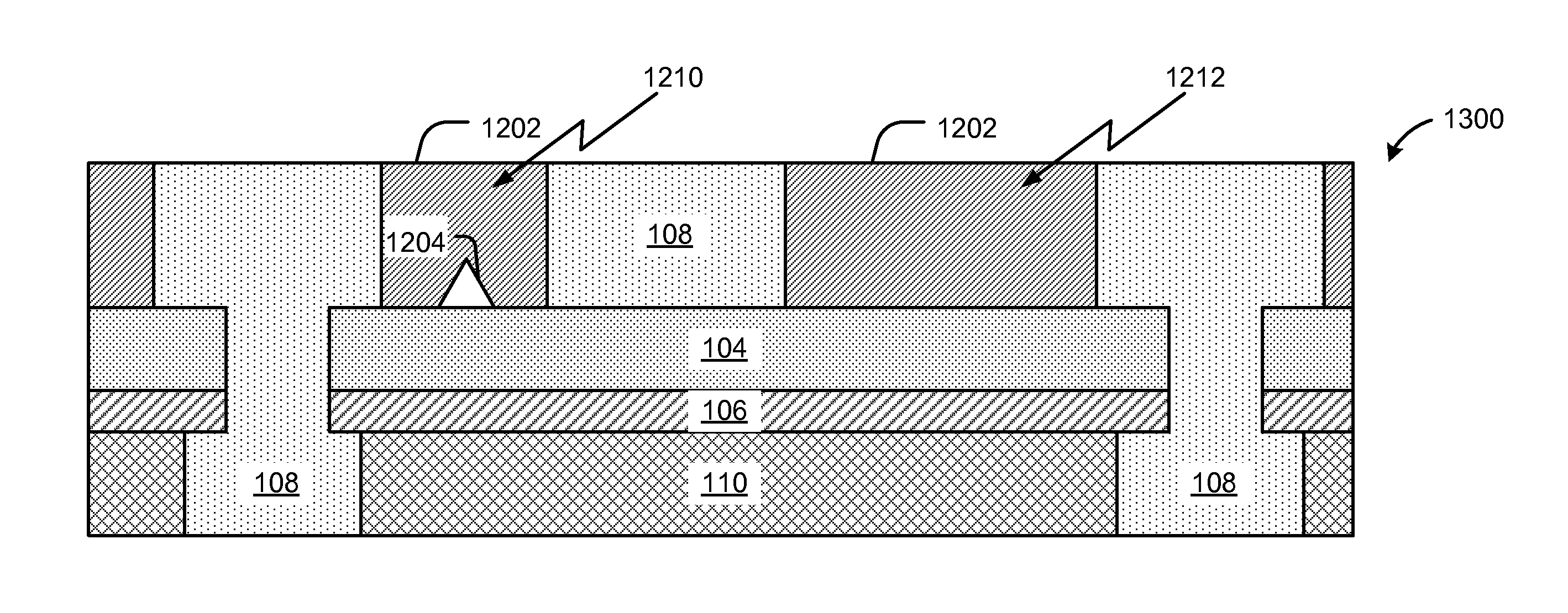
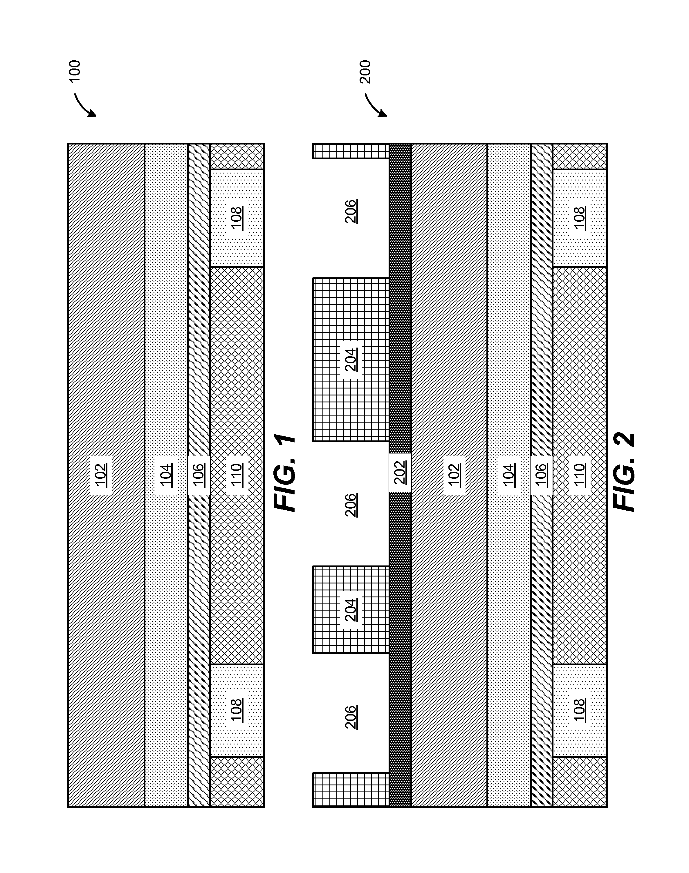
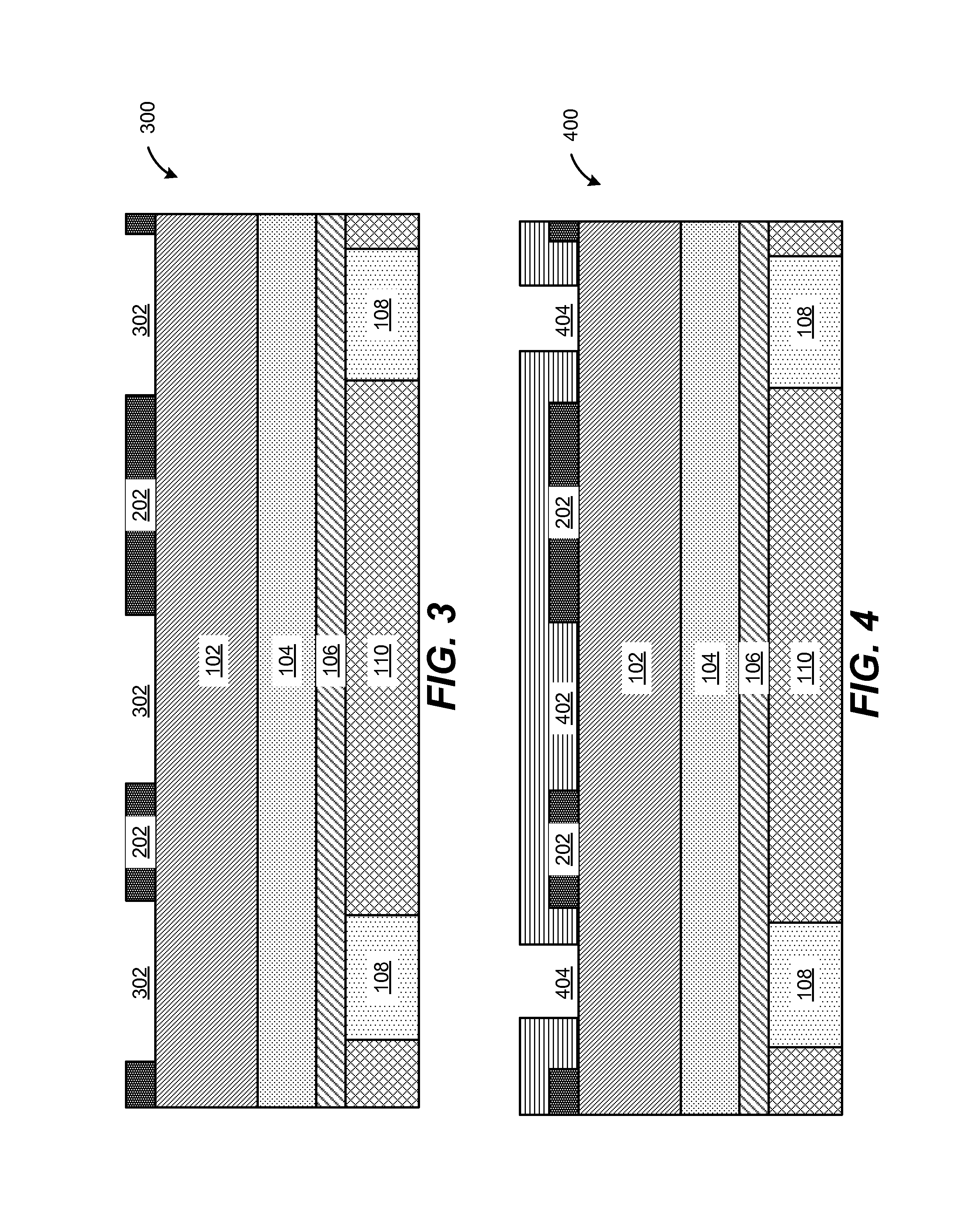
[0028]FIGS. 1-13, as described herein, illustrate a side view of a structure as formed during particular stages of one or more methods of fabricating one or more electronic devices. In a particular embodiment, each structure illustrated in FIGS. 1-13 is formed during particular stages of fabricating an electronic device (e.g., a semiconductor device). A method of fabricating one or more of the structures illustrated in FIGS. 1-13 may correspond to a back end of line (BEOL) process (e.g., forming interconnects between components such as capacitors, inductors, transistors, diodes, resistors, or other integrated circuit devices). Accordingly, other processes may also be performed that are not specifically described, such as front end of line (FEOL) processes (e.g., forming components), packaging, or other BEOL processes. One or more of the structures illustrated in FIGS. 1-13 may correspond to a semiconductor device, a passive-on-glass device, an integrated circuit device, or another e...


PUM

PropertyMeasurementUnit
threshold distanceaaaaaaaaaa
temperatureaaaaaaaaaa
dielectric constantaaaaaaaaaa

Abstract

A method includes forming an electronic device structure including a substrate, an oxide layer, and a first low-k layer. The method also includes forming openings by patterning the oxide layer, filling the openings with a conductive material to form conductive structures within the openings, and removing the oxide layer using the first low-k layer as an etch stop layer. The conductive structures contact the first low-k layer. Removing the oxide layer includes performing a chemical vapor etch process with respect to the oxide layer to form an etch byproduct and removing the etch byproduct. The method includes forming a second low-k layer using a deposition process that causes the second low-k layer to define one or more cavities. Each cavity is defined between a first conductive structure and an adjacent conductive structure, the first and second conductive structures have a spacing therebetween that is smaller than a threshold distance.

Description

I. CROSS-REFERENCE TO RELATED APPLICATIONS[0001]The present application claims priority from commonly owned U.S. Provisional Patent Application No. 61 / 952,384 filed Mar. 13, 2014 and entitled “CAPACITANCE REDUCTION SYSTEM,” the contents of which are expressly incorporated herein by reference in their entirety.II. FIELD[0002]The present disclosure is generally related to systems and methods of forming a reduced capacitance device.III. DESCRIPTION OF RELATED ART[0003]Advances in technology have resulted in smaller and more powerful computing devices. For example, there currently exist a variety of portable personal computing devices, including wireless computing devices, such as portable wireless telephones, personal digital assistants (PDAs), and paging devices that are small, lightweight, and easily carried by users. More specifically, portable wireless telephones, such as cellular telephones and internet protocol (IP) telephones, can communicate voice and data packets over wireless...

Claims


Application Information

Patent Timeline
Patent Type & Authority Applications(United States)
IPC IPC(8): H01L21/768H01L21/311
CPCH01L21/76879H01L21/31138H01L21/7682H01L21/76885H01L21/31116H01L21/31144
Inventor XU, JEFFREY JUNHAOZHU, JOHN JIANHONGSONG, STANLEY SEUNGCHULRIM, KERNYEAP, CHOH FEI
Owner QUALCOMM INC
Why Eureka
Try Eureka