Bright and clean x-ray source for x-ray based metrology

a x-ray source and metrology technology, applied in the direction of x-ray tubes, material analysis using wave/particle radiation, instruments, etc., can solve the problems of optical radiation not being able to penetrate to the bottom layer, difficult to characterize, and difficult to achieve the effect of high brightness and low contamination levels

Active Publication Date: 2022-04-26
KLA CORP
View PDF79 Cites 0 Cited by
  • Summary
  • Abstract
  • Description
  • Claims
  • Application Information

AI Technical Summary

Benefits of technology

[0014]Methods and systems for x-ray based semiconductor metrology utilizing a clean, hard X-ray illumination source are described herein. More specifically, a laser produced plasma (LPP) light source generates high brightness (i.e., greater than 1013 photons / (sec·'mm2·mrad2) hard x-ray illumination having energy in a range of 25,000 to 30,000 electron volts. To achieve such high brightness, the LPP light source directs a highly focused, very short duration laser beam to a dense Xenon target in a liquid or solid state. The interaction of the focused laser pulse with the high density Xenon target ignites a plasma. Radiation from the plasma is collected by collection optics and is directed to a specimen under measurement. The resulting plasma emission is relatively clean because of the use of a non-metallic target material. As a result, the plasma chamber and optical elements within the plasma chamber are subject to very low levels of contamination due to the plasma.

Problems solved by technology

As devices (e.g., logic and memory devices) move toward smaller nanometer-scale dimensions, characterization becomes more difficult.
Devices incorporating complex three-dimensional geometry and materials with diverse physical properties contribute to characterization difficulty.
For example, modern memory structures are often high-aspect ratio, three-dimensional structures that make it difficult for optical radiation to penetrate to the bottom layers.
Optical metrology tools utilizing infrared to visible light can penetrate many layers of translucent materials, but longer wavelengths that provide good depth of penetration do not provide sufficient sensitivity to small anomalies.
As a result, the parameters characterizing the target often cannot be reliably decoupled with available measurements.
Optical radiation is often unable to penetrate layers constructed of these materials.
As a result, measurements with thin-film scatterometry tools such as ellipsometers or reflectometers are becoming increasingly challenging.
However, these approaches have not reliably overcome fundamental challenges associated with measurement of many advanced targets (e.g., complex 3D structures, structures smaller than 10 nm, structures employing opaque materials) and measurement applications (e.g., line edge roughness and line width roughness measurements).
Unfortunately, the resulting illumination is low brightness due to heating and evaporation of anode material by the high energy electron beam.
However, the liquid metal anode material does evaporate and form a metal vapor that may limit x-ray source lifetime.
In some examples, the metal vapor diffuses into the cathode region and contaminates the cathode, reducing cathode lifetime and system output.
In some examples, the metal vapor diffuses into the electron beam acceleration region causing high-voltage breakdowns.
While substantial radiance improvements are obtained with laser sustained plasmas, the temperature of these plasmas is generally limited by the photophysical and kinetic processes within these lamps.
Excimer emission can be arranged in laser sustained plasmas for wavelength emission at 171 nm (e.g., xenon excimer emission), but these sources are typically narrow band, limited in power, and limited in radiance.
As a consequence, a simple gas mixture in a high pressure bulb is only able to sustain wavelength coverage above 200 nm with sufficient radiance and average power to support high throughput, high resolution metrology.
In some examples, solid electrode targets are employed, but low repetition rate, electrode erosion, and large plasma size result in low brightness and short lifetime, limiting their effectivity for x-ray based semiconductor metrology.
However, the resulting radiation is relatively low energy (92.6 electron volts), which severely limits the utility of these illumination sources in metrology applications.
As a result, the plasma chamber and optical elements within the plasma chamber are subject to very low levels of contamination due to the plasma.

Method used


Image

  • Bright and clean x-ray source for x-ray based metrology
  • Bright and clean x-ray source for x-ray based metrology
  • Bright and clean x-ray source for x-ray based metrology

Examples


Embodiment Construction

[0024]Reference will now be made in detail to background examples and some embodiments of the invention, examples of which are illustrated in the accompanying drawings.

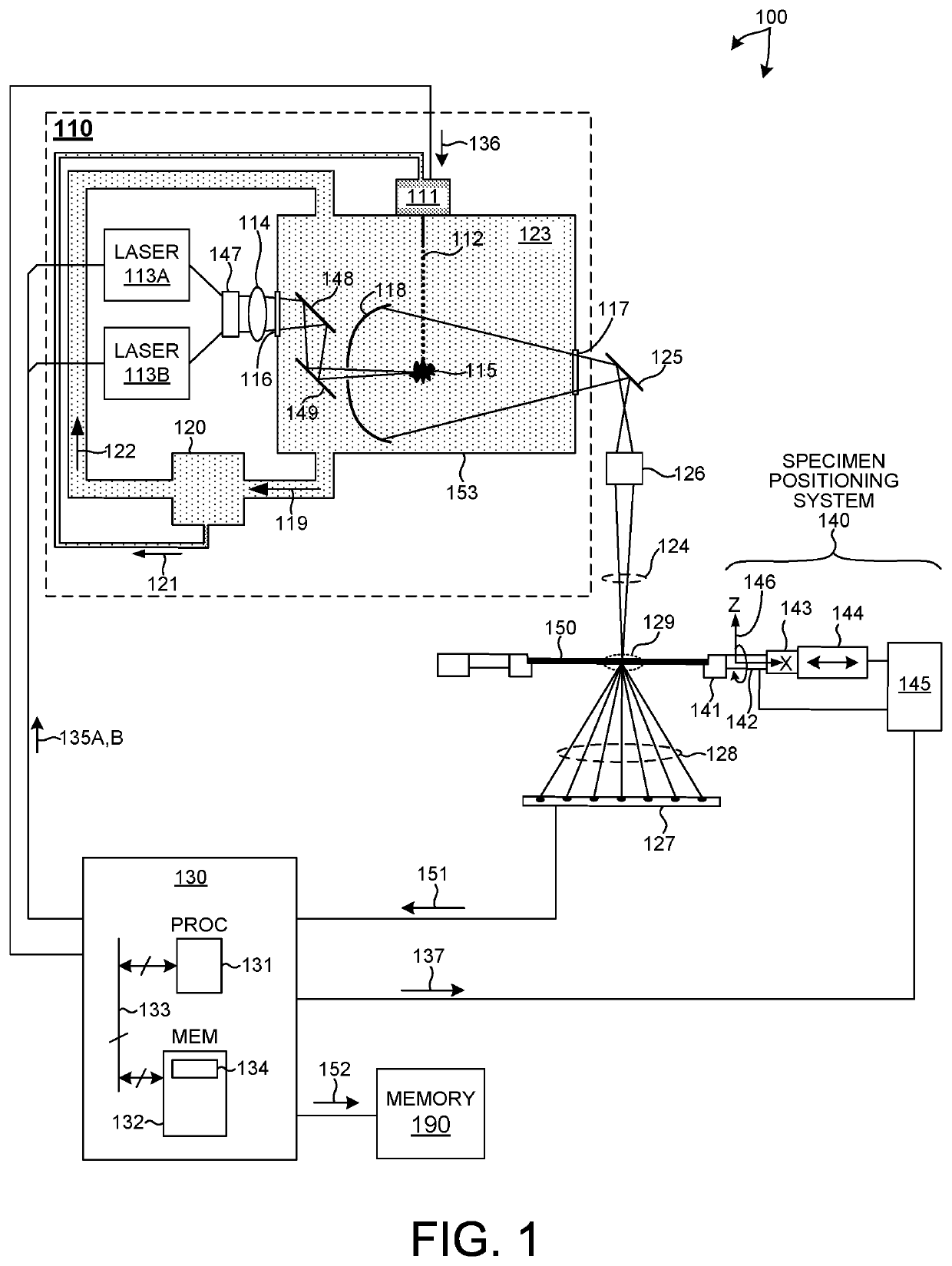
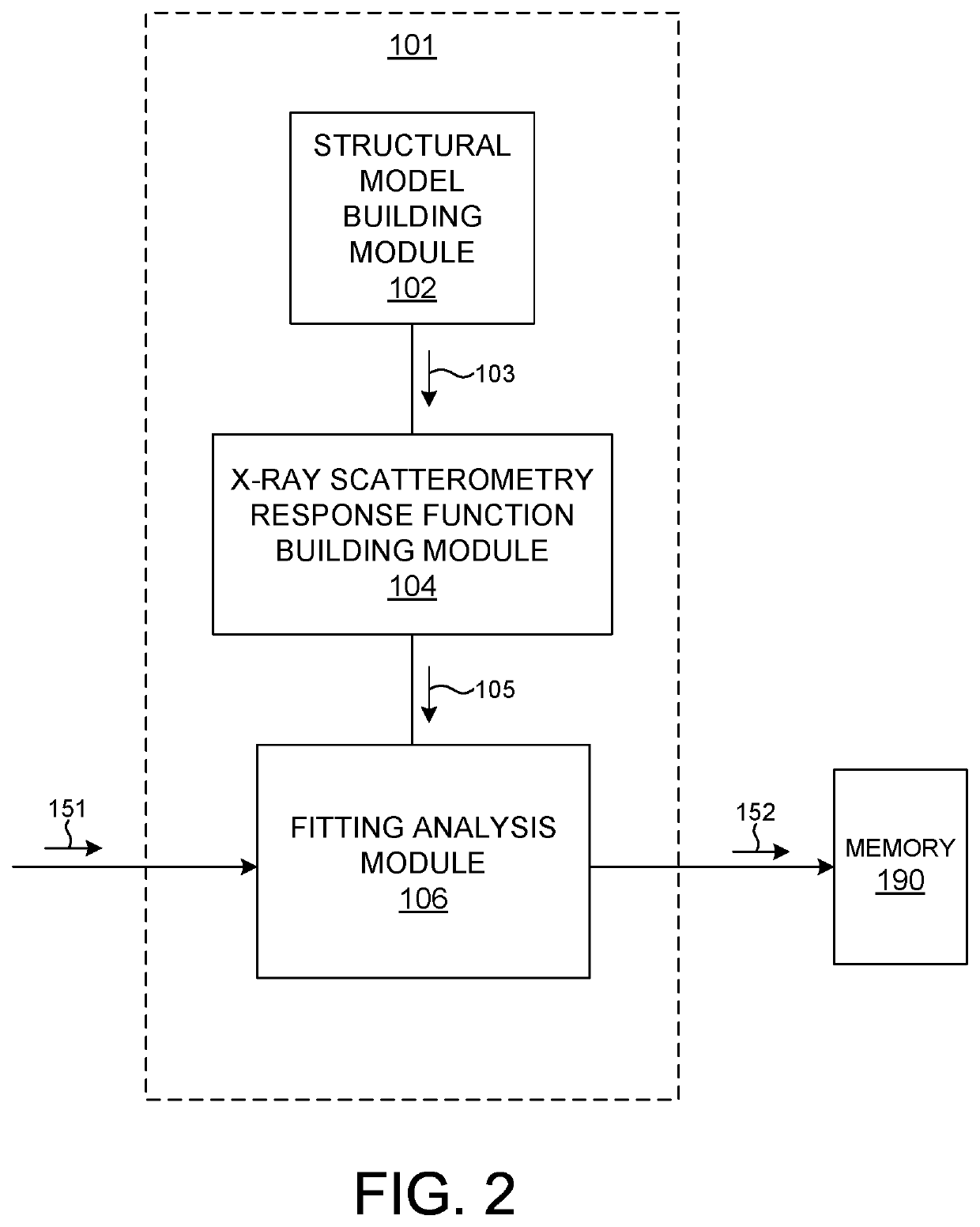
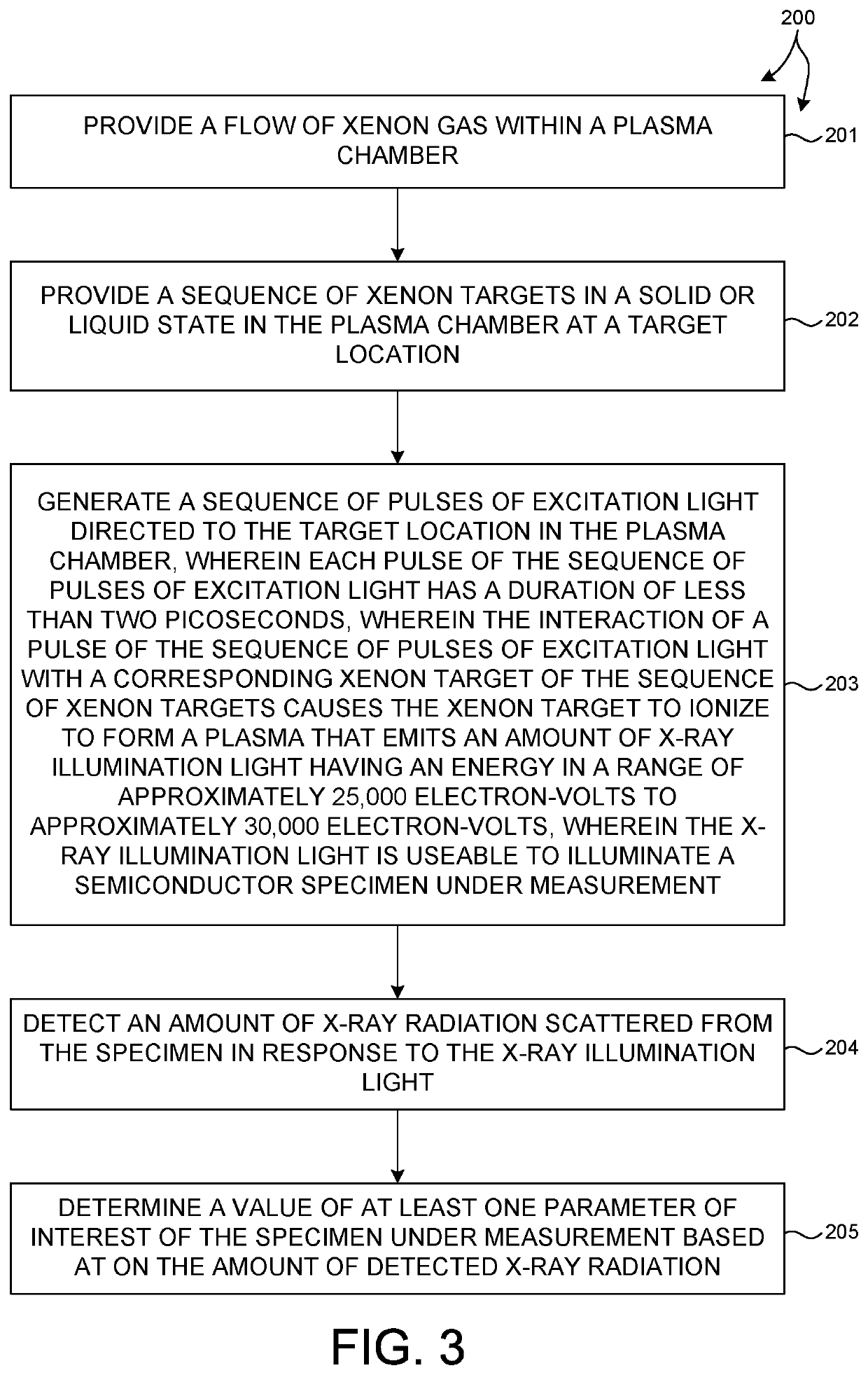
[0025]Methods and systems for x-ray based semiconductor metrology utilizing a clean, hard X-ray illumination source are described herein. More specifically, a laser produced plasma (LPP) light source generates high brightness (i.e., greater than 1013 photons / (sec·mm2·mrad2) hard x-ray illumination having energy in a range of 25,000 to 30,000 electron volts. To achieve such high brightness, the LPP light source directs a highly focused (e.g., less than 10 micrometer illumination spot on target), very short duration (e.g., less than 2 picoseconds) laser beam to a dense Xenon target in a liquid or solid state. The interaction of the focused laser pulse with the high density Xenon target ignites a plasma. Radiation from the plasma is collected by collection optics and is directed to a specimen under measurement. The resul...


PUM

PropertyMeasurementUnit
pressureaaaaaaaaaa
pressureaaaaaaaaaa
distanceaaaaaaaaaa

Abstract

Methods and systems for x-ray based semiconductor metrology utilizing a clean, hard X-ray illumination source are described herein. More specifically, a laser produced plasma light source generates high brightness, hard x-ray illumination having energy in a range of 25,000 to 30,000 electron volts. To achieve high brightness, a highly focused, very short duration laser beam is focused onto a dense Xenon target in a liquid or solid state. The interaction of the focused laser pulse with the high density Xenon target ignites a plasma. Radiation from the plasma is collected by collection optics and is directed to a specimen under measurement. The resulting plasma emission is relatively clean because of the use of a non-metallic target material. The plasma chamber is filled with Xenon gas to further protect optical elements from contamination. In some embodiments, evaporated Xenon from the plasma chamber is recycled back to the Xenon target generator.

Description

TECHNICAL FIELD[0001]The described embodiments relate to x-ray laser produced plasma radiation sources and systems for x-ray metrology and inspection.BACKGROUND INFORMATION[0002]Semiconductor devices such as logic and memory devices are typically fabricated by a sequence of processing steps applied to a substrate or wafer. The various features and multiple structural levels of the semiconductor devices are formed by these processing steps. For example, lithography among others is one semiconductor fabrication process that involves generating a pattern on a semiconductor wafer. Additional examples of semiconductor fabrication processes include, but are not limited to, chemical-mechanical polishing, etch, deposition, and ion implantation. Multiple semiconductor devices may be fabricated on a single semiconductor wafer and then separated into individual semiconductor devices.[0003]Metrology processes are used at various steps during a semiconductor manufacturing process to detect defec...

Claims


Application Information

Patent Timeline
Patent Type & Authority Patents(United States)
IPC IPC(8): H05G2/00G01N23/20008G01N23/201
CPCH05G2/008G01N23/201G01N23/20008H05G2/006H05G2/005
Inventor KHODYKIN, OLEG
Owner KLA CORP
Why Eureka
Try Eureka