Arc-sprayed shield for pre-sputter etching chamber

a shield and sputter technology, applied in the field of etching, can solve the problems of reducing the overall product yield, limiting the application of electrically conductive materials, and using high pressure, and achieve the effect of high degree of roughness

Inactive Publication Date: 2005-09-13
TAIWAN SEMICON MFG CO LTD
View PDF8 Cites 5 Cited by
  • Summary
  • Abstract
  • Description
  • Claims
  • Application Information

AI Technical Summary

Benefits of technology

[0015]These objects have been achieved by coating the full interior of the sputtering shield with a layer of an arc-sprayed material such as aluminum, said layer being possessed of a high degree of roughness.

Problems solved by technology

DC (direct current) sputter-etching is similar, but is limited to electrically conductive material, which RF sputter-etching is not.
This use of high pressure, and particularly high power, is known to have certain undesirable side effects, notably the generation of fine dust particles, some of which find their way onto the surface that was sputter-etched.
Any particulate matter of this type, if allowed to settle on the surface of an integrated circuit during the course of its manufacture, has a high probabilty of destroying said circuit, thus reducing the overall product yield.

Method used


Image

  • Arc-sprayed shield for pre-sputter etching chamber
  • Arc-sprayed shield for pre-sputter etching chamber
  • Arc-sprayed shield for pre-sputter etching chamber

Examples


Embodiment Construction

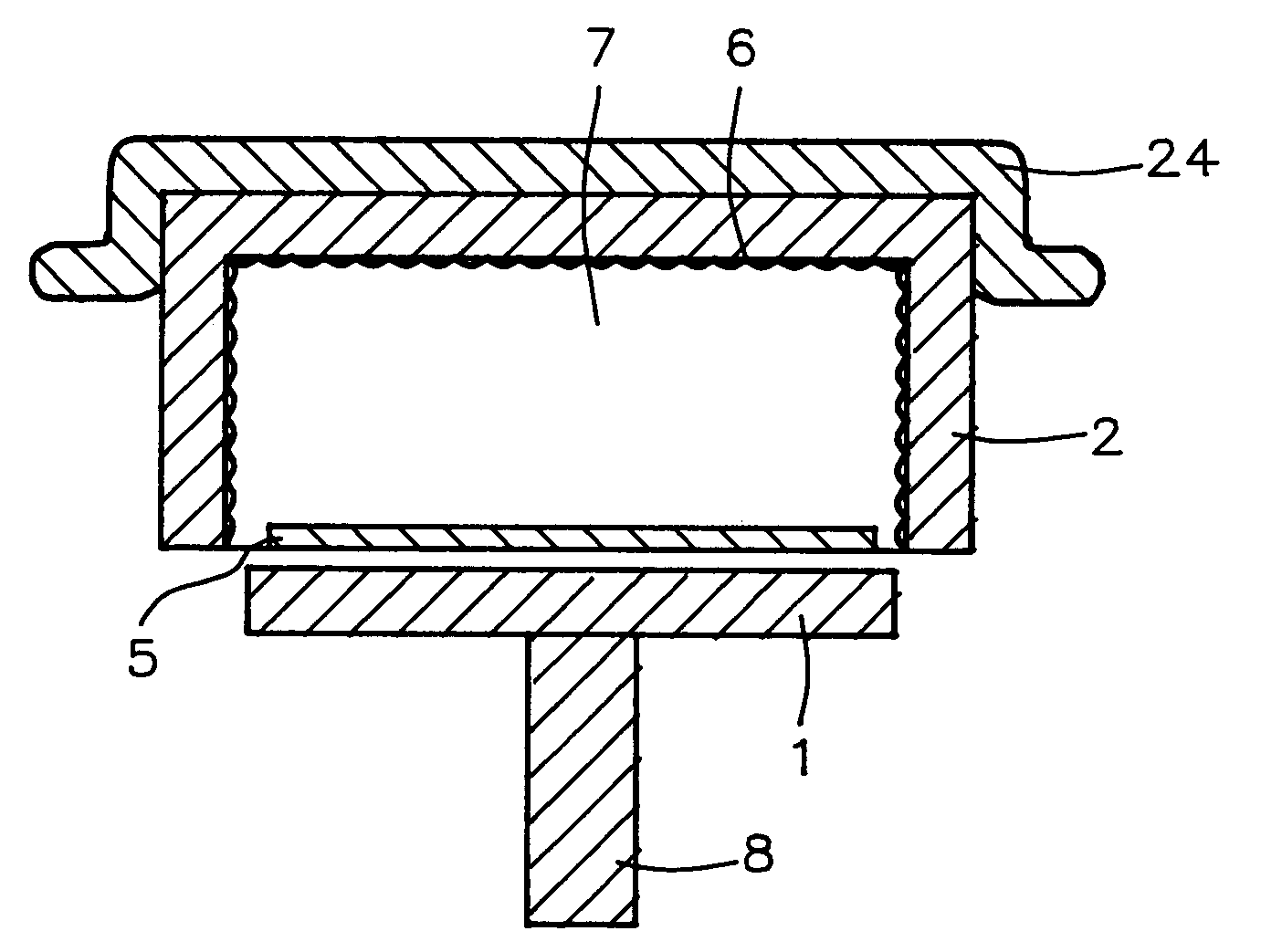
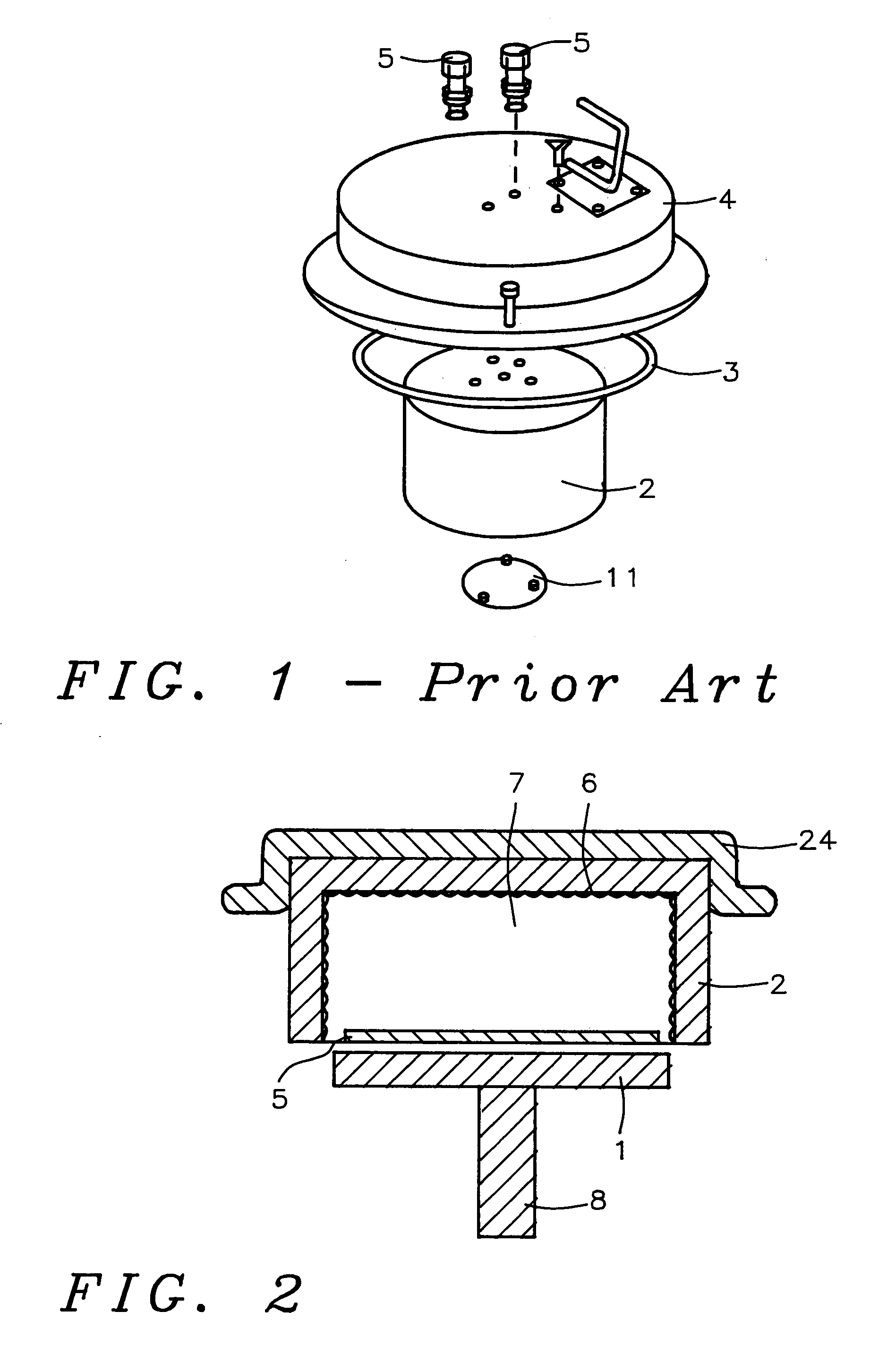
[0021]Referring now to FIG. 2, we show in schematic cross-section, the key parts (relative to the present invention) of the sputter-etcher shown in FIG. 1. A substrate holder 8, supporting substrate 5, is positioned just inside sputtering shield 2. Lid 24 (simplified here so the gas admission control and the gas baffle are not shown) sits on top of shield 2. When an RF glow discharge is initiated in region 7 (by applying an RF voltage between about 1,550 and 1,750 volts), material from the surface of 5 is removed at a steady rate which is typically about 200 Angstrom units per minute. However, the present invention, as we will describe it below, is applicable to a wide range of deposition rates—from about 100 to about 250 Angstrom units per minute.

[0022]A key feature of the present invention is layer 6 which covers the entire inside surface of sputtering shield 2. The inside surface of layer 6, whose thickness may be anything from about 120 microns to about 180 microns (a value of 1...


PUM

PropertyMeasurementUnit
roughnessaaaaaaaaaa
thicknessaaaaaaaaaa
pressureaaaaaaaaaa

Abstract

Contamination due to deposited particulate matter has been greatly reduced in single wafer sputter-etchers by coating the full interior of the sputtering shield with a layer of an arc-sprayed material such as aluminum, said layer being possessed of a high degree of surface roughness. The method for forming the coating of arc-sprayed aluminum is described and data comparing particulate contaminant count and product yield before and after the adoption of the present invention, are presented.

Description

BACKGROUND OF THE INVENTION[0001](1) Field of the Invention[0002]The invention relates to the general field of etching by non chemical means, particularly RF sputter-etching.[0003](2) Description of the Prior Art[0004]RF (radio frequency) sputter-etching is a universal etching technique, although the actual rate at which material gets removed does vary from one material to another. DC (direct current) sputter-etching is similar, but is limited to electrically conductive material, which RF sputter-etching is not. The basic setup is to provide two electrodes—a substrate holder and a sputtering shield, immerse them in gas at low pressure and apply an RF voltage between them.[0005]FIG. 1 shows an exploded isometric view of part of a standard sputter-etcher of this type, in this case Electrotech's model MS6210 which was used in the development and reduction to practice of the present invention. During use, silicone oil cooled substrate holder 1 (shown in FIG. 2) is positioned just inside...

Claims


Application Information

Patent Timeline
Patent Type & Authority Patents(United States)
IPC IPC(8): C23C14/34H01L21/00
CPCH01J37/34H01J37/3411H01J37/3438H01J37/3476
Inventor LIN, CHENG-KUNYANG, CHIN-SHIENCHEN, CHUAN-HUAI
Owner TAIWAN SEMICON MFG CO LTD
Why Eureka
Try Eureka