Electronic device and gas barrier film manufacturing method

a technology of electronic devices and gas barrier films, which is applied in the direction of film/foil adhesives, applications, other domestic articles, etc., can solve the problems of the above-described gas barrier film losing its flatness, and the gas barrier film of the electronic device not giving sufficient performance to serve, etc., to achieve high gas barrier properties and durability, high flexibility, and high adhesion to the resin substrate

Inactive Publication Date: 2015-10-08
KONICA MINOLTA INC
View PDF0 Cites 5 Cited by
  • Summary
  • Abstract
  • Description
  • Claims
  • Application Information

AI Technical Summary

Benefits of technology

[0010]Specifically, the advantageous effects of the present invention can be achieved by the following aspects:
[0011]1. An electronic device comprising a gas barrier film including, in sequence:
[0036]The aspects according to the present invention described above can provide an electronic device including a gas barrier film exhibiting high gas-barrier properties and durability (flatness and dark-spot resistance) in the use in a high-temperature and high-humidity environment and a method of manufacturing such a gas barrier film.
[0039]Such a gas barrier layer disposed on the resin substrate and having elemental (atomic) distribution profiles continuously changing across the thickness of the gas barrier layer can exhibit high adhesion to the resin substrate and high flexibility, as well as high gas barrier properties. Unfortunately, an electronic device including a gas barrier film having such a gas barrier layer loses flatness because the layers of the gas barrier film have different contraction rates, and the contraction rate of the gas barrier layer is relatively higher than that of the resin substrate. Specifically, an electronic device including a resin film substrate having a thickness in a range of 15 to 150 μm is more prone to lose the flatness. The loss in flatness of the electronic device is remarkably observed specifically after being kept under a high-temperature and high-humidity environment for a long period. For instance, an organic electroluminescent device as an electronic device including such a gas barrier film may generate dark spots due to the loss in flatness, which leads to malfunction of the organic electroluminescent device.
[0040]The inventor of the present invention has eagerly examined these problems from several points of view, and has found that a gas barrier film which is a laminate of the gas barrier layer and an inorganic polymer layer having a predetermined contraction rate is resistant to the loss in the flatness, and that an electronic device including such a gas barrier film can exhibit high durability (flatness and dark-spot resistance).
[0042]Even if the inorganic polymer layer having a contraction rate defined herein is laminated on the gas barrier layer having a substantially homogeneous elemental profile, the loss in flatness of an electronic device is unavoidable because of a difference in contraction between the gas barrier layer and the inorganic polymer layer: specifically, the contraction of the inorganic polymer layer having a predetermined contraction rate cannot compensate for the contraction of the gas barrier layer having a homogeneous elemental profile, and thus cannot prevent loss in flatness of the electronic device, but rather impairs the flatness of the gas barrier layer. This leads to significantly low durability of the electronic device.

Problems solved by technology

Unfortunately, there are no gas barrier films that give sufficient performance to serve as these flexible electronic devices which should have significantly high gas-barrier properties at the glass substrate level.
It is found that the above-described gas barrier film of the electronic device loses its flatness when being exposed to such a high-temperature environment.

Method used


Image

  • Electronic device and gas barrier film manufacturing method
  • Electronic device and gas barrier film manufacturing method
  • Electronic device and gas barrier film manufacturing method

Examples


examples

[0337]The present invention will now be described in further detail with reference to non-limiting examples. Throughout the examples, the terms “part” and “%” respectively represent “part by mass” and “mass %” unless otherwise mentioned.

[0338]>

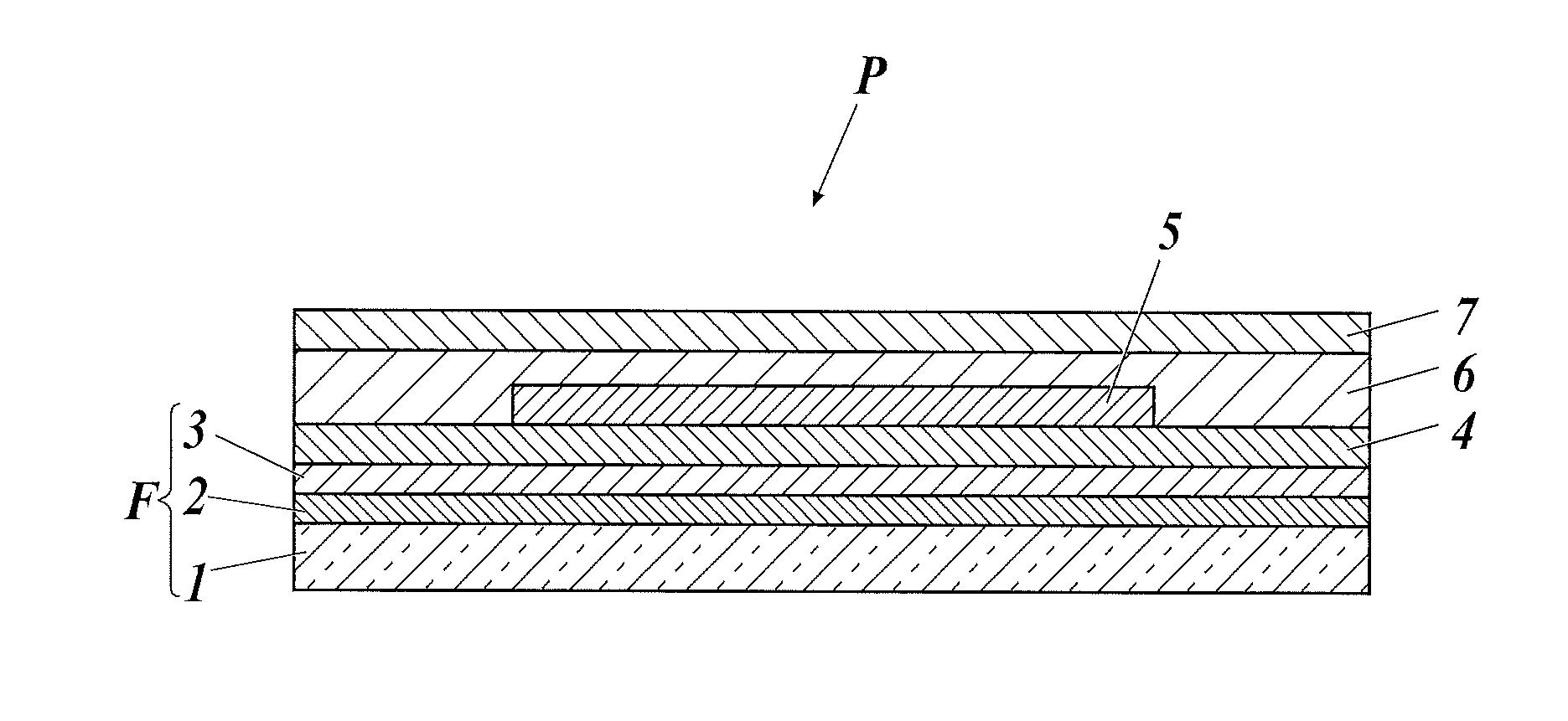
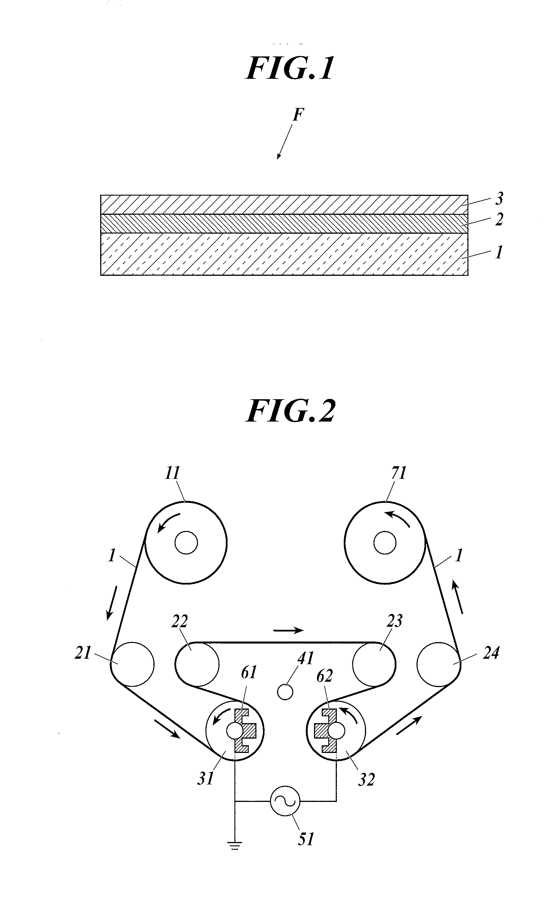
[0339][Production of Gas Barrier Film 1: Comparative Example]

[0340](Preparation of Resin Substrate)

[0341]A resin substrate used was a biaxially stretched polyethylene naphthalate (PEN) film (thickness: 100 μm, width: 350 mm, Teonex Q65FA, available from Teijin DuPont Films Japan Limited).

[0342](Formation of Anchor Layer)

[0343]A UV-curable organic / inorganic hybrid hard coat material, OPSTARZ7501, available from JSR Corporation, was applied with a wire bar to form a coating layer onto an easy adhesion surface of the resin substrate such that the dried coating layer had a thickness of 4 μm. The coating layer was dried at 80° C. for 3 minutes. The dried coating layer was then cured into an anchor layer with a high-pressure mercury lamp under a con...


PUM

PropertyMeasurementUnit
thicknessaaaaaaaaaa
wavelengthaaaaaaaaaa
temperatureaaaaaaaaaa

Abstract

An electronic device may be provided which is superior in gas barrier performance and robustness (flatness and dark spot resistance), and a gas barrier film fabrication method may be provided.

Description

TECHNICAL FIELD[0001]The present invention relates to an electronic device including a gas barrier film and a method of manufacturing the gas barrier film.BACKGROUND ART[0002]A conventional gas barrier film that is a laminate of a plastic (film) substrate and several layers including metal oxide films composed of, for example, aluminum oxide, magnesium oxide, and silicon oxide are widely used for wrapping food, industrial, and pharmaceutical products which should be blocked from gases, such as moisture vapor and oxygen, in order to prevent alteration of the products.[0003]Many studies have been conducted on development in use of gas barrier films in the form of flexible electronic devices, for example, flexible solar cell devices, flexible organic electroluminescent (EL) devices, and flexible liquid crystal displays, in addition to wrapping materials. Unfortunately, there are no gas barrier films that give sufficient performance to serve as these flexible electronic devices which sh...

Claims


Application Information

Patent Timeline
Patent Type & Authority Applications(United States)
IPC IPC(8): C23C16/40C23C16/54C23C16/513
CPCY10T428/266Y10T428/31663C23C16/545C23C16/513C23C16/402C23C16/50C23C16/30B32B27/08B32B27/283B32B2255/10B32B2307/7242B32B2457/00B32B2605/00H10K50/844
Inventor SUZUKI, ISSEI
Owner KONICA MINOLTA INC
Why Eureka
Try Eureka