Method and system for optical proximity correction (OPC)

a technology of optical proximity and optical proximity correction, applied in the direction of originals for photomechanical treatment, design optimisation/simulation, instruments, etc., can solve the problems of degrading image fidelity and poor quality of fabricated semiconductor devices

Active Publication Date: 2015-10-08
SEMICON MFG INT (SHANGHAI) CORP
View PDF3 Cites 9 Cited by
  • Summary
  • Abstract
  • Description
  • Claims
  • Application Information

AI Technical Summary

Benefits of technology

[0005]One aspect of the present disclosure includes an Optical Proximity Correction (OPC) method for compensating the Optical Proximity Effect (OPE) influence. The method include providing a substrate having at least one semiconductor structure and with a plurality of regions, providing a target pattern to be formed on the substrate, and respectively obtaining aerial

Problems solved by technology

This may generate dimension variation between the fabricated pattern and the designed mask and may

Method used


Image

  • Method and system for optical proximity correction (OPC)
  • Method and system for optical proximity correction (OPC)
  • Method and system for optical proximity correction (OPC)

Examples


Embodiment Construction

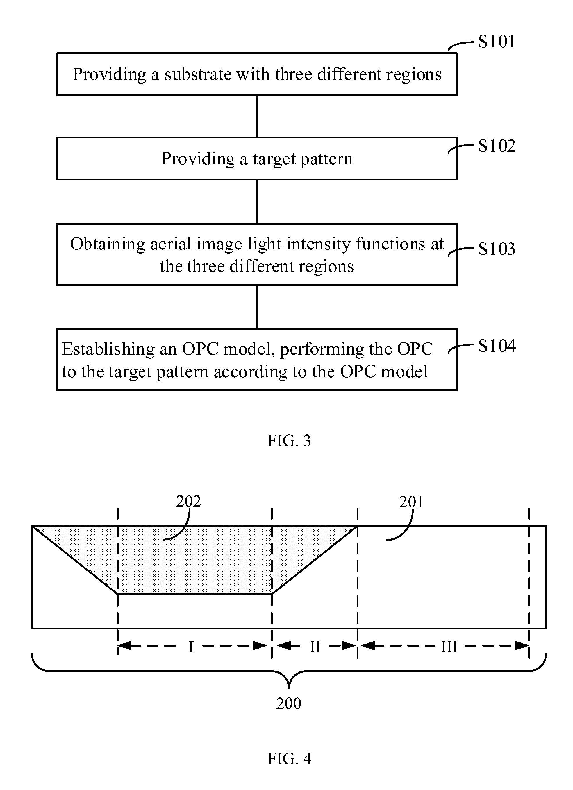
[0014]Reference will now be made in detail to exemplary embodiments of the invention, which are illustrated in the accompanying drawings. Wherever possible, the same reference numbers will be used throughout the drawings to refer to the same or like parts. It is apparent that the described embodiments are some but not all of the embodiments of the present invention. Based on the disclosed embodiment, persons of ordinary skill in the art may derive other embodiments consistent with the present disclosure, all of which are within the scope of the present invention.

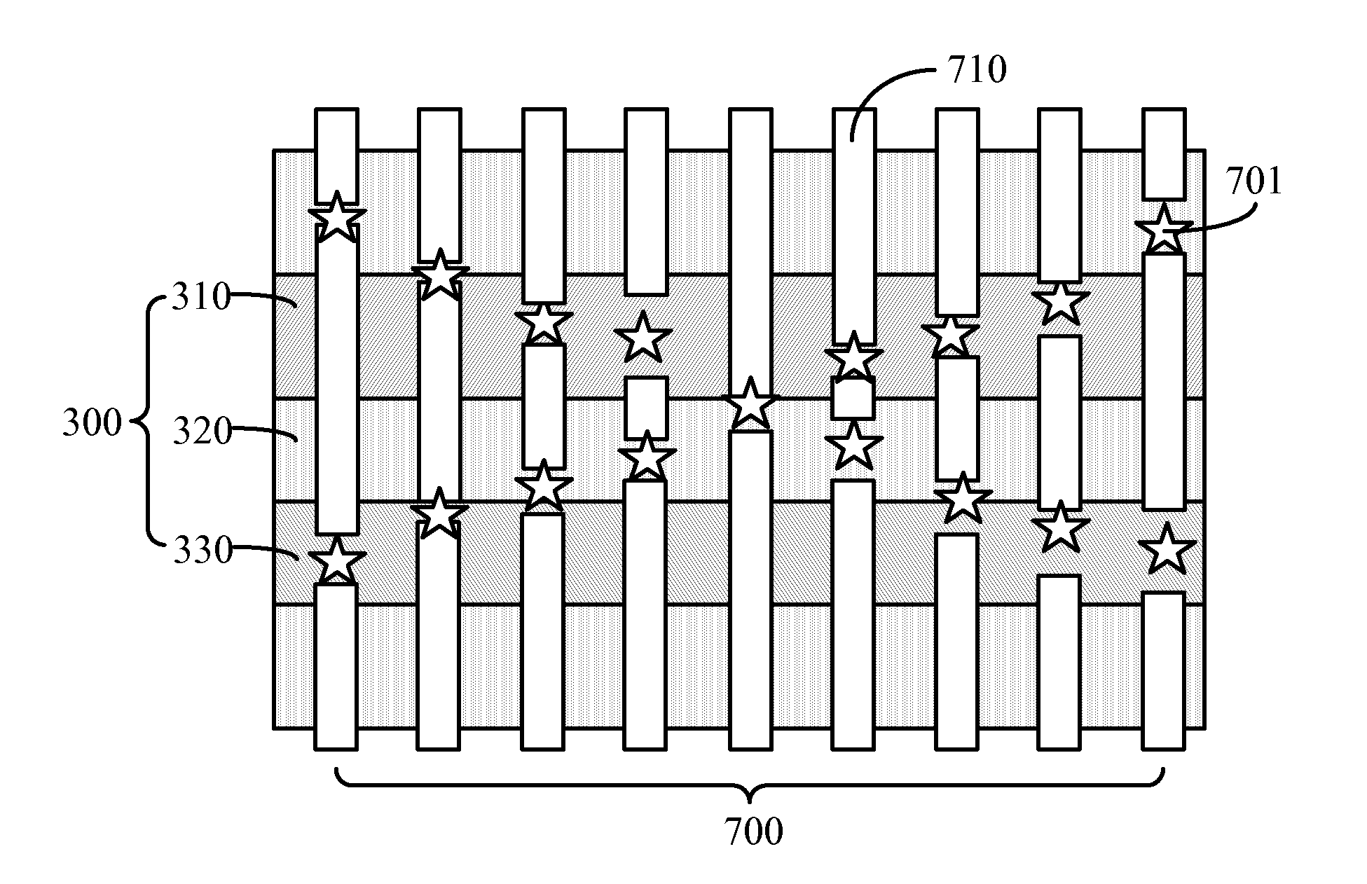
[0015]As mentioned in the background section, when a semiconductor substrate has certain structure such as STIs, there may be some variations between the finally formed patterns on the substrate and the target patterns.

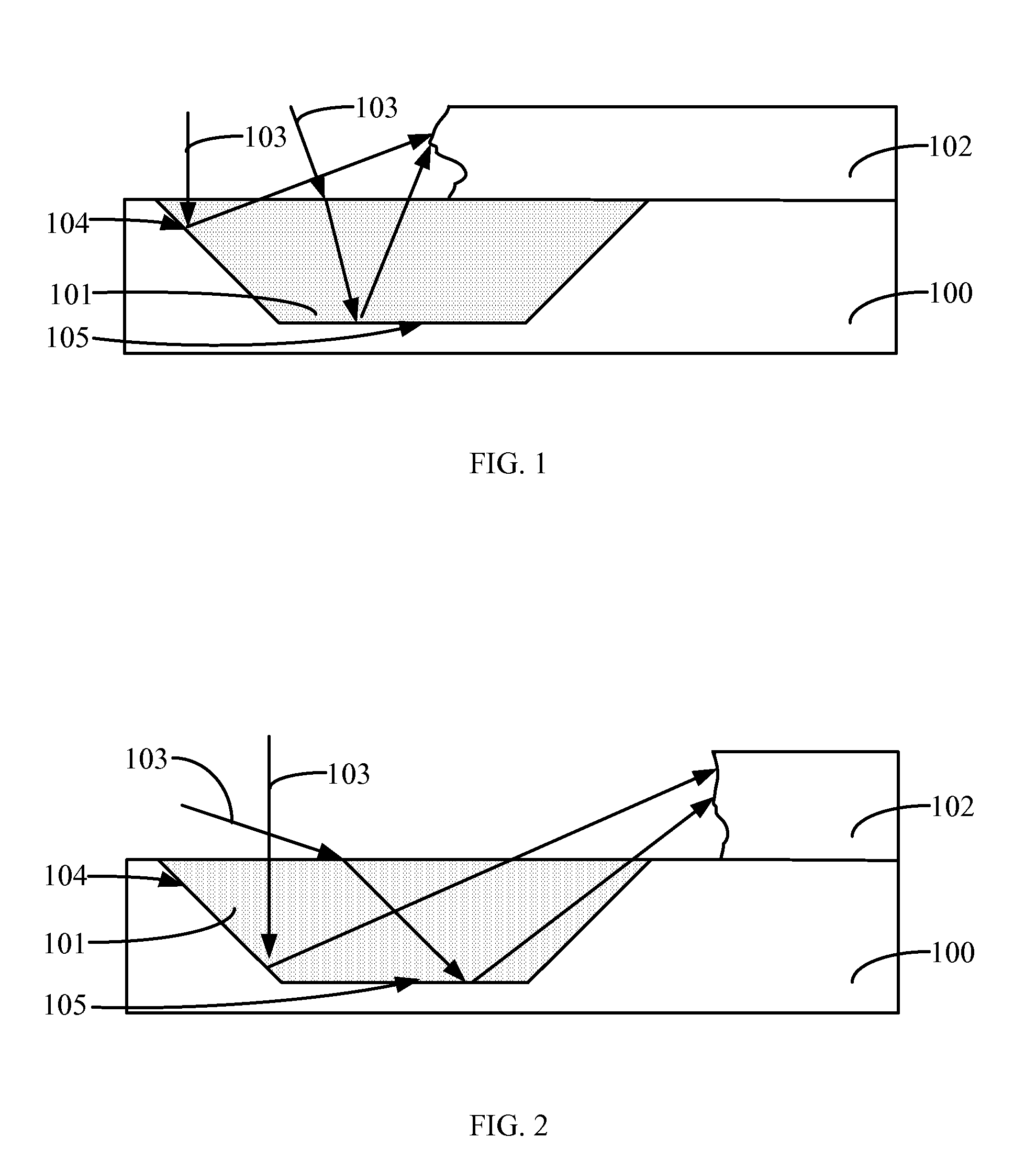
[0016]As shown in FIGS. 1-2, to form a photoresist layer having a target pattern, a semiconductor substrate 100 is provided. The substrate 100 has an insulator structure 101, and a photoresist layer is formed ...


PUM


Abstract

An Optical Proximity Correction (OPC) method is provided for compensating the Optical Proximity Effect (OPE) influence. The method include providing a substrate having at least one semiconductor structure and with a plurality of regions, providing a target pattern to be formed on the substrate, and respectively obtaining aerial image light intensity functions of the plurality of regions of the substrate. The method also includes establishing an OPC model based on the aerial image light intensity functions of the plurality of regions, and performing an OPC process to the target pattern by using the OPC model to adjust the target pattern factoring in optical effect of the plurality of regions.

Description

CROSS-REFERENCES TO RELATED APPLICATIONS[0001]This application claims the priority of Chinese patent application no. CN201410131227.X, filed on Apr. 2, 2014, the entire contents of all of which are incorporated herein by reference.FIELD OF THE INVENTION[0002]The present invention relates to the field of semiconductor manufacturing processes technology and, more particularly, relates to an Optical Proximity Correction (OPC) method and a method for optimizing an OPC model.BACKGROUND[0003]With rapid development on semiconductor manufacturing processes technology, feature size of semiconductor devices continues to shrink to meet the requirements for miniaturization, low power consumption, and high-degree-integration. As the feature size decreasing, light diffraction effect in photolithography becomes more and more obvious. This may generate dimension variation between the fabricated pattern and the designed mask and may degrade image fidelity. This phenomena is known as the Optical Prox...

Claims


Application Information

Patent Timeline
IPC IPC(8): G03F1/36G06F17/50
CPCG06F17/5009G03F1/36G06F30/20
Inventor CHENG, RENQIANGWANG, HUI
Owner SEMICON MFG INT (SHANGHAI) CORP
Why Eureka
Try Eureka