Spectral mapping of photo emission

a technology of emission spectrum and photon emission, which is applied in the direction of optically investigating flaws/contamination, material analysis, instruments, etc., can solve the problems of complicated dut probing, malfunctioning devices, and becoming more difficult to identify malfunctioning devices, so as to maximize efficiency and minimize power

Active Publication Date: 2015-10-15
DCG SYST
View PDF1 Cites 4 Cited by
  • Summary
  • Abstract
  • Description
  • Claims
  • Application Information

AI Technical Summary

Benefits of technology

[0022]The concept behind the disclosed embodiments is the use of transmission grating to enable insertion of the grating in the optical path of the tester in registration with, and without disrupting, the image of the emission itself. By proper choice of a transmission grating, e.g., a proper transmission blazed grating, the emission can be imaged without the grating and thereafter the grating can be inserted in the optical path without disrupting the view of the emission and while preserving the registration of the emission spot. This is achieved, in part, by choosing the transmission grating such that the zero order is the integrated emission and the first order is a diffraction of the emission spot. When choosing appropriate blazed grating, it is optimized to achieve maximum efficiency at the first diffraction order and minimize power at the higher orders. The blazed grating is made of material that is transparent at 800-2500 nm wavelengths and the blaze angle of the blazed grating is configured to have maximum power at first order for wavelength or between 800 nm and 2500 nm, although depending on the sensor used, the blazed grating is configured to have maximum power at first order for wavelength or between 800 nm and 1600 nm instead.
[0023]According to a variation embodiment, the transmissive grating is made as a rotatable grating to identify, localize and classify faulty devices in the IC. The grating is used to break the detected light into its frequency components. This helps in identifying and classifying the defects. The subject inventors discovered that beneficial information can be obtained by imaging the IC using different rotational orientation of the grating. This effect is used to help identify, localize and classify the defects. Since the techniques and embodiments described herein are particularly beneficial in emission microscopy, both static and dynamic, much of the remainder of the description refers to emission microscopy.
[0024]In essence, while in standard emission systems the collected light appears circular, inserting a diffraction element in the light collection path causes the spectra of the emission to be imaged and appear generally in a linear form, according to the amount of diffraction. Using the transmissive diffraction grating, a zero order is projected in registration with the image of the emission spot, and the first order is projected to the side of the emission spot. Thus, the user can identify the spot from which the first order diffraction corresponds to. Using these images, the user can analyze the image of the first order diffraction and determining whether the spot of the zero order diffraction is faulty. When using rotatable transmissive grating, the orientation of the spectra may appear different, i.e., the axis of the spectra oriented at different angle, depending on the rotation of the diffraction element. Additionally, the shape of the spectra itself may look different, e.g., as a linear streak, as a “comet tail,” as a “teardrop,” etc., depending on the type of fault. All these phenomena can help in identifying, localizing and classifying faulty devices. Also, when the emission appears as a streak, the distribution of frequencies along the axis of the streak can help identifying, localizing and classifying faulty devices.

Problems solved by technology

Several issues complicate probing of DUT's, especially in view of shrinking dimensions following Moore's Law.
Among the issues is identifying malfunctioning devices.
That is, with the shrinking dimensions and lowering of operational voltage, it becomes more difficult to identify malfunctioning devices, either because the light emission is too faint or because light modulation is to small compared to background noise.
Another issue is localizing the faulty device.
That is, even if it is determined that a certain area of the DUT includes a faulty device, due to the density of devices it is difficult to know exactly where or which is the faulty device.
For example a faulty transistor may be overloaded or saturated.
In this respect, one type of fault is when a transistor that continues to conduct as in an overloaded state.

Method used


Image

  • Spectral mapping of photo emission
  • Spectral mapping of photo emission
  • Spectral mapping of photo emission

Examples


Embodiment Construction

[0041]Various embodiments of the present invention provide apparatus and method for non-invasive, non-contact method for probing active transistors within a selected area of the DUT. The described methodologies augment the prior art system by enhancing the ability to identify faulty devices or identify working transistors in a wrong state because of surrounding issues like shorts, due to process / design errors, provide improved ability to localize the faulty device even in a highly dense area, and provide method for classifying the fault to assist in failure analysis. In fact, embodiments of the invention also enable identifying thermal emission. For example, conductor line resistance emission can be identified, i.e., not transistor or device but just resistive metal line emitting heat. The curve or spectral profile in that case is even more exponential than the NMOS in saturation. Various embodiments showing examples of implementation of the system will now be described.
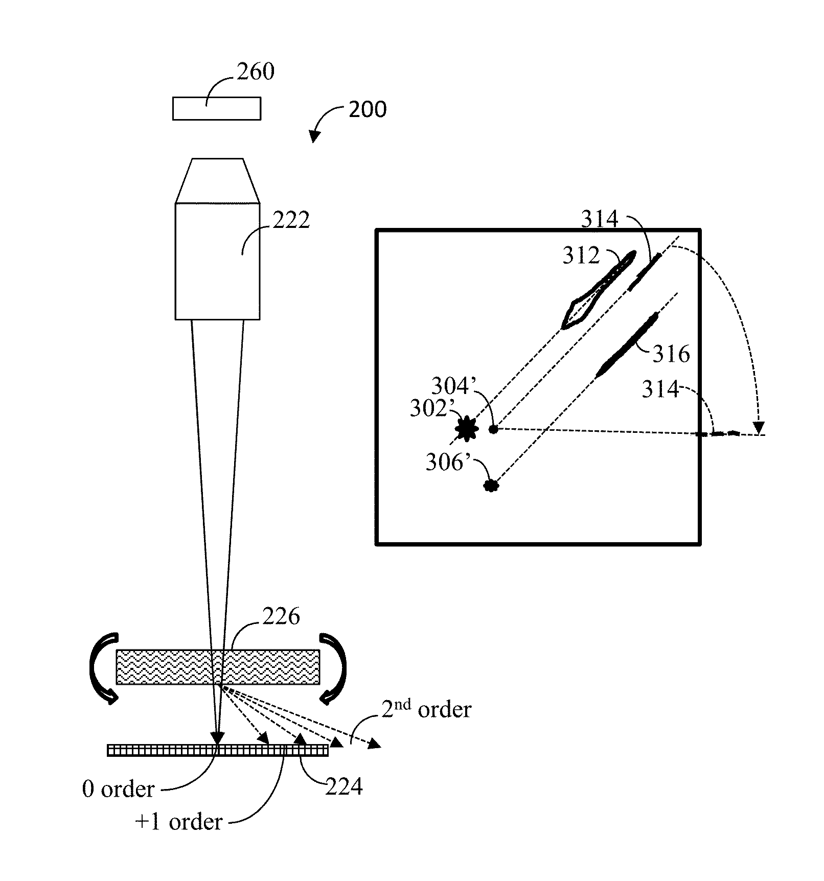
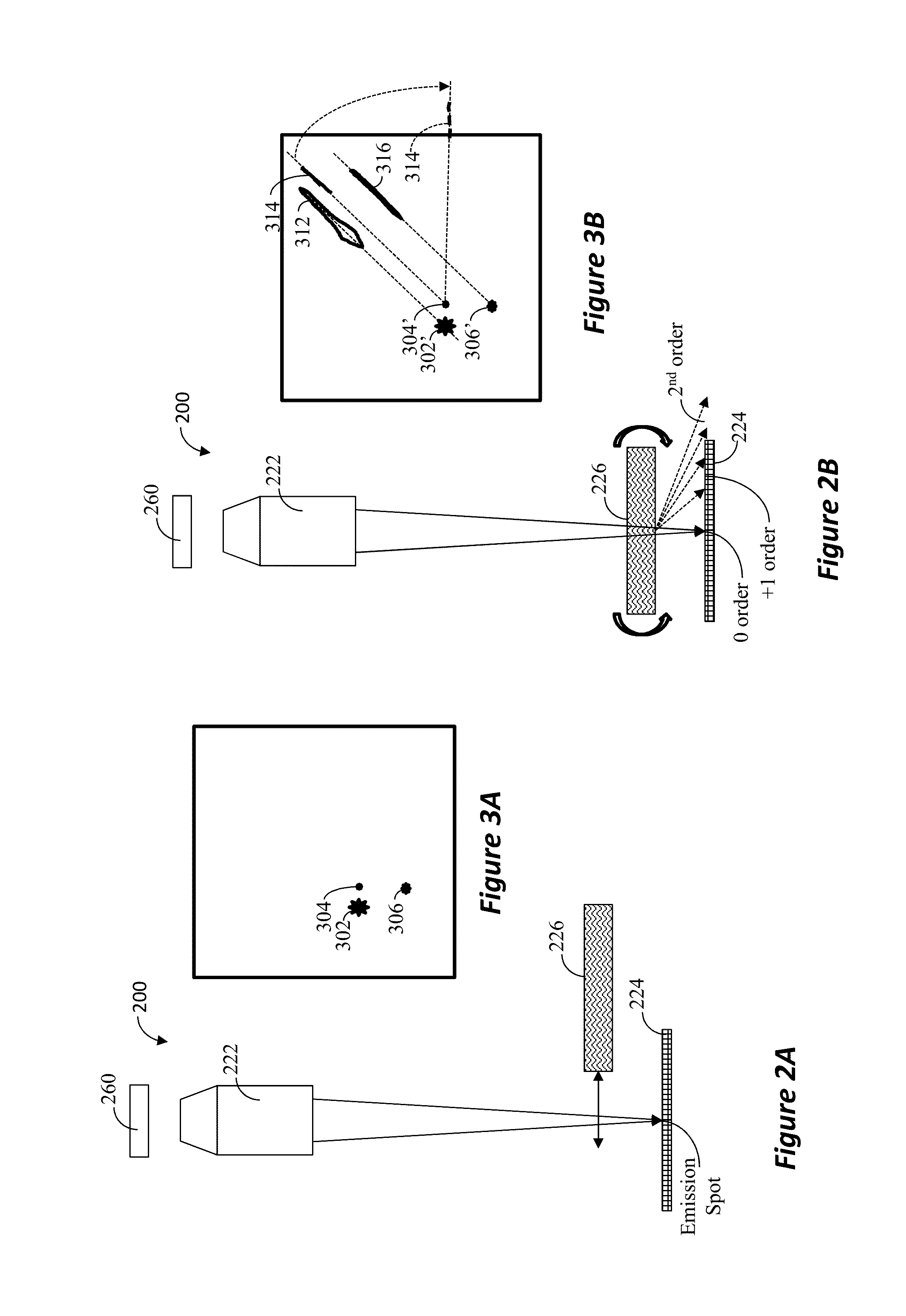
[0042]FIG. 2...


PUM

PropertyMeasurementUnit
wavelengthsaaaaaaaaaa
frequencyaaaaaaaaaa

Abstract

An apparatus and method for optical probing of a DUT is disclosed. The system enables identifying, localizing and classifying faulty devices within the DUT. A selected area of the DUT is imaged while the DUT is receiving test signals, which may be static or dynamic, i.e., causing certain of the active devices to modulate. Light from the DUT is collected and is passed through a transparent diffracting grating prior to imaging it by a sensor and converting it into an electrical signal. The resulting image includes the zero order and first order diffraction of the grating. The grating is configured such that the zero order is in registration with emission sites imaged when the grating is outside the optical path.

Description

CROSS-REFERENCE TO RELATED APPLICATION[0001]This application is related to and claims priority from U.S. Provisional Application Ser. No. 61 / 978,173, filed on Apr. 10, 2014, the disclosure of which is hereby incorporated herein by reference in its entirety.BACKGROUND[0002]1. Field[0003]The present invention relates to an apparatus and method for performing emission spectra analysis of photon emission from a device under test (DUT). The invention relates to identifying, localizing, and classifying malfunctioning elements within the DUT.[0004]2. Related Art[0005]Probing systems have been used in the art for testing and debugging integrated circuit (IC) designs and layouts. Various emission and laser-based systems for probing IC's are known in the prior art. While some description of the prior art is provided herein, the reader is encouraged to also review U.S. Pat. No. 5,208,648, 5,220,403, 5,940,545, 6,943,572, 7,012,537, 7,038,442, 7,224,828, and 7,323,862, which are incorporated he...

Claims


Application Information

Patent Timeline
Patent Type & Authority Applications(United States)
IPC IPC(8): G01N21/95G01N21/956
CPCG01N21/956G01N21/9505G01N21/66G01N21/9501G01R31/311
Inventor DESLANDES, HERVEREVERDY, ANTOINEPARRASSIN, THIERRY
Owner DCG SYST
Why Eureka
Try Eureka