Semiconductor device and method of manufacturing the same

a technology of semiconductors and semiconductors, applied in the direction of transistors, chemical vapor deposition coatings, coatings, etc., can solve the problems of reducing the reliability of the transistor, and reducing the thickness of the barrier film or the seed layer

Inactive Publication Date: 2015-10-15
LONGITUDE SEMICON S A R L
View PDF3 Cites 20 Cited by
  • Summary
  • Abstract
  • Description
  • Claims
  • Application Information

AI Technical Summary

Benefits of technology

[0006]Meanwhile, if the width of the trench structure becomes smaller as a result of miniaturization of the semiconductor device, the space in which to embed the bulk W film becomes narrower, and there is a risk that it will cease to exist. In order to maintain a space in which to form the bulk W film, it is conceivable to employ methods in which the thickness of the barrier film or the seed layer is reduced. However, according to investigations conducted by the inventors, if the thickness of the barrier film is reduced to less than 5 nm, problems arise in that there is a degradation of the transistor characteristics, and reliability cannot be ensured. The cause of this is thought to be that reducing the thickness of the barrier film results in a deterioration in the barrier properties wit...

Problems solved by technology

Reaction by-products such as F and HF, which may damage the silicon substrate or the gate insulating film, are generated when these films are being deposited.
Meanwhile, if the width of the trench structure becomes smaller as a result of miniaturization of the semiconductor device, the space in which to embed the bulk W film becomes narrower, and there is a risk that it will cease to exist.
However, according to investigations conducted by the inventors, if the t...

Method used


Image

  • Semiconductor device and method of manufacturing the same
  • Semiconductor device and method of manufacturing the same
  • Semiconductor device and method of manufacturing the same

Examples


embodiment 1

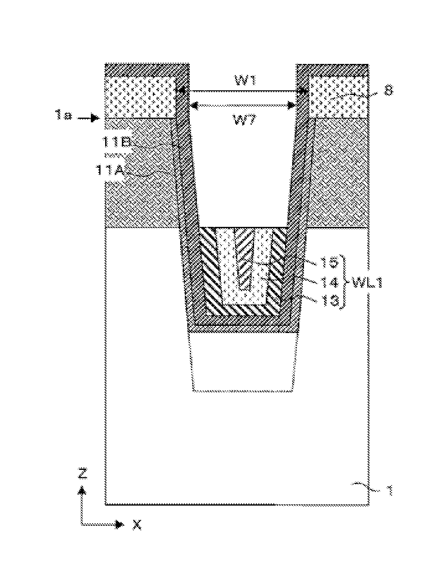
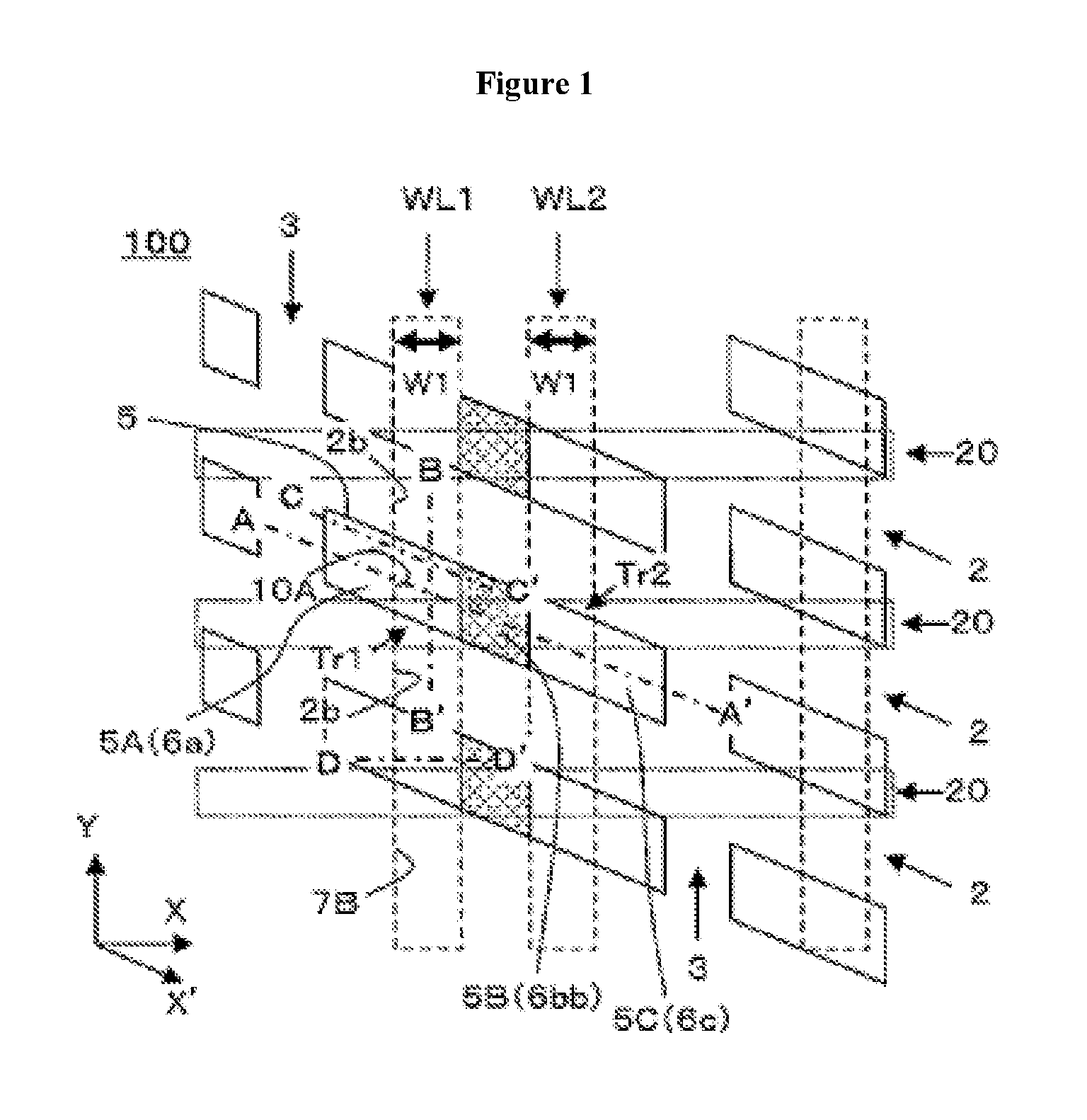
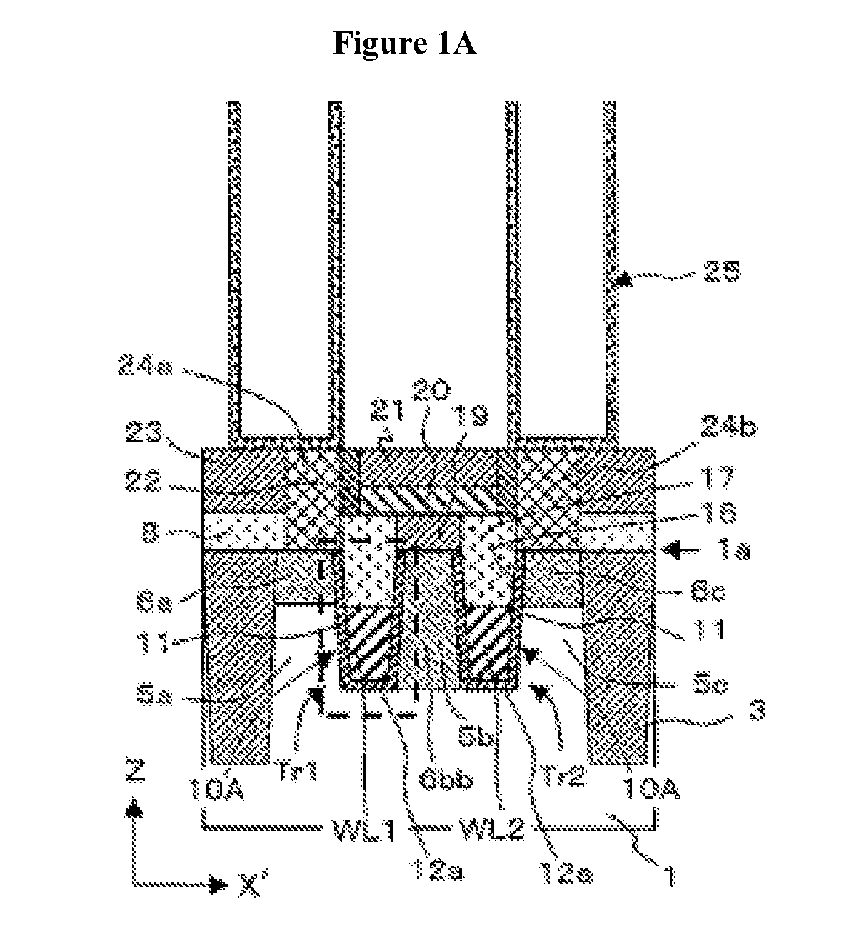
[0050]The configuration of the semiconductor device in this embodiment will first be described with reference to FIG. 1, FIG. 1A, FIG. 1B, FIG. 1C, FIG. 1D and FIG. 1E. FIG. 1 is a plan view illustrating the planar layout of the constituent elements of the semiconductor device, FIG. 1A is a cross-sectional view through the line A-A′ in FIG. 1, FIG. 1B is a cross-sectional view through the line B-B′, FIG. 1C is a cross-sectional view through the line C-C′, and FIG. 1D is a cross-sectional view through the line D-D′. Further, FIG. 1E is a cut-away perspective view of the semiconductor device, used to describe the internal structure of the semiconductor device according to this mode of embodiment. It should be noted that the dimensions of the parts in the drawings are not necessarily proportional to the dimensions of the actual parts. Further, the scale of the drawings is not necessarily common. Further, some parts are omitted from each drawing for convenience of description, and in so...

embodiment 2

[0088]A method of manufacturing the semiconductor device discussed hereinabove will now be described with reference to FIG. 2 to FIG. 15A. Drawings having a drawing number without a letter appended thereto are plan views of each step. Further, drawings having a drawing number with the letter A appended are cross-sectional views through the line A-A′ illustrated in the corresponding plan view, or cross-sectional views in a location corresponding to the line A-A′, and drawings with the letter B appended are cross-sectional views through the line B-B′ illustrated in the corresponding plan view, or cross-sectional views in a location corresponding to the line B-B′.

[0089]Referring to FIG. 2, FIG. 2A and FIG. 2B, first a step of forming element isolation regions and active regions is implemented.

[0090]In a semiconductor substrate 1 comprising a p-type silicon single crystal, first element isolation grooves having side surfaces 2a and extending in the X′-direction (first direction), and se...

embodiment 3

[0143]In embodiment 2 a method was described in which the barrier insulating film 11B is formed using thermal nitriding. In this embodiment 3, a method in which the barrier insulating film 11B having a thickness TG2 of 3 nm is formed by ALD, in other words by film deposition, is described with reference to FIG. 16D.

[0144]In the same way as in FIG. 5 in embodiment 2, the word trench 7B (10A) is formed using as a mask the masking film 8 which has an opening width W1 of 25 nm. Then, as illustrated in FIG. 16D, the first insulating film 11A having a thickness TG1 of 2 nm is formed by the same thermal oxidation method as in embodiment 2. The barrier insulating film 11B having a thickness TG2 of 3 nm is then formed by ALD.

[0145]A silicon nitride film (SiN), a silicon oxynitride film (SiON), an aluminum nitride film (AlN), an aluminum oxynitride film (AlON) or the like can be used as the barrier insulating film 11B formed by ALD. Each of these is an amorphous crystalline film. Further, in ...


PUM

PropertyMeasurementUnit
Thicknessaaaaaaaaaa
Thicknessaaaaaaaaaa
aaaaaaaaaa

Abstract

This semiconductor device comprises: a trench that is provided in a semiconductor substrate; an insulating film that covers the inner surface of the trench; and a buried wiring line that fills up the lower part within the trench and is in contact with the insulating film. A barrier insulating film is arranged at least at the interface between the insulating film and the buried wiring line.

Description

TECHNICAL FIELD[0001]The present invention relates to a semiconductor device and a method for manufacturing the same, and more specifically relates to a semiconductor device containing transistors provided with an embedded metal gate electrode, and a method for manufacturing the same.BACKGROUND ART[0002]In semiconductor devices such as DRAMs (Dynamic Random Access Memory), miniaturization has occurred in conjunction with the adoption of memory arrays comprising transistors having an embedded word line construction, in which the active regions of memory cells are formed in a line pattern, trenches extending in a direction which intersects the active regions are formed in a substrate, and word lines (gate electrodes) are embedded in the trenches (patent literature article 1). If F is the minimum processing dimension, then in F30 and F25 generation DRAMs the trenches are formed to a width of approximately 30 nm and 25 nm respectively.[0003]The embedded word lines are formed using a met...

Claims


Application Information

Patent Timeline
IPC IPC(8): H01L27/108H01L29/423H01L21/3213H01L29/51H01L21/02H01L21/768
CPCH01L27/10891H01L21/02255H01L27/10876H01L27/1085H01L27/10823H01L21/02247H01L21/76877H01L21/76871H01L21/76843H01L21/0223H01L21/32133H01L21/0217H01L21/0214H01L21/02178H01L21/0228H01L29/511H01L29/517H01L29/518H01L29/4236H01L21/02252H01L27/10885H01L21/3065H01L21/76224C23C16/308C23C16/345C23C16/45525H10B12/315H10B12/34H10B12/053H10B12/488H10B12/03H10B12/482
Inventor NAKATA, SHINICHI
Owner LONGITUDE SEMICON S A R L
Why Eureka
Try Eureka