Method and applications of thin-film membrane transfer

a thin-film membrane and transfer printing technology, applied in the direction of instruments, force measurement by measuring optical property variation, active medium materials, etc., can solve the problems of limited work within the existing silicon semiconductor-based framework, and achieve the effect of optimizing device performance, reducing applied voltage, and increasing tunable rang

Active Publication Date: 2015-10-29
MASSACHUSETTS INST OF TECH
View PDF5 Cites 35 Cited by
  • Summary
  • Abstract
  • Description
  • Claims
  • Application Information

AI Technical Summary

Problems solved by technology

However, the conventional methods are limited to working within the existing silicon semiconductor-based framework.

Method used


Image

  • Method and applications of thin-film membrane transfer
  • Method and applications of thin-film membrane transfer
  • Method and applications of thin-film membrane transfer

Examples


Embodiment Construction

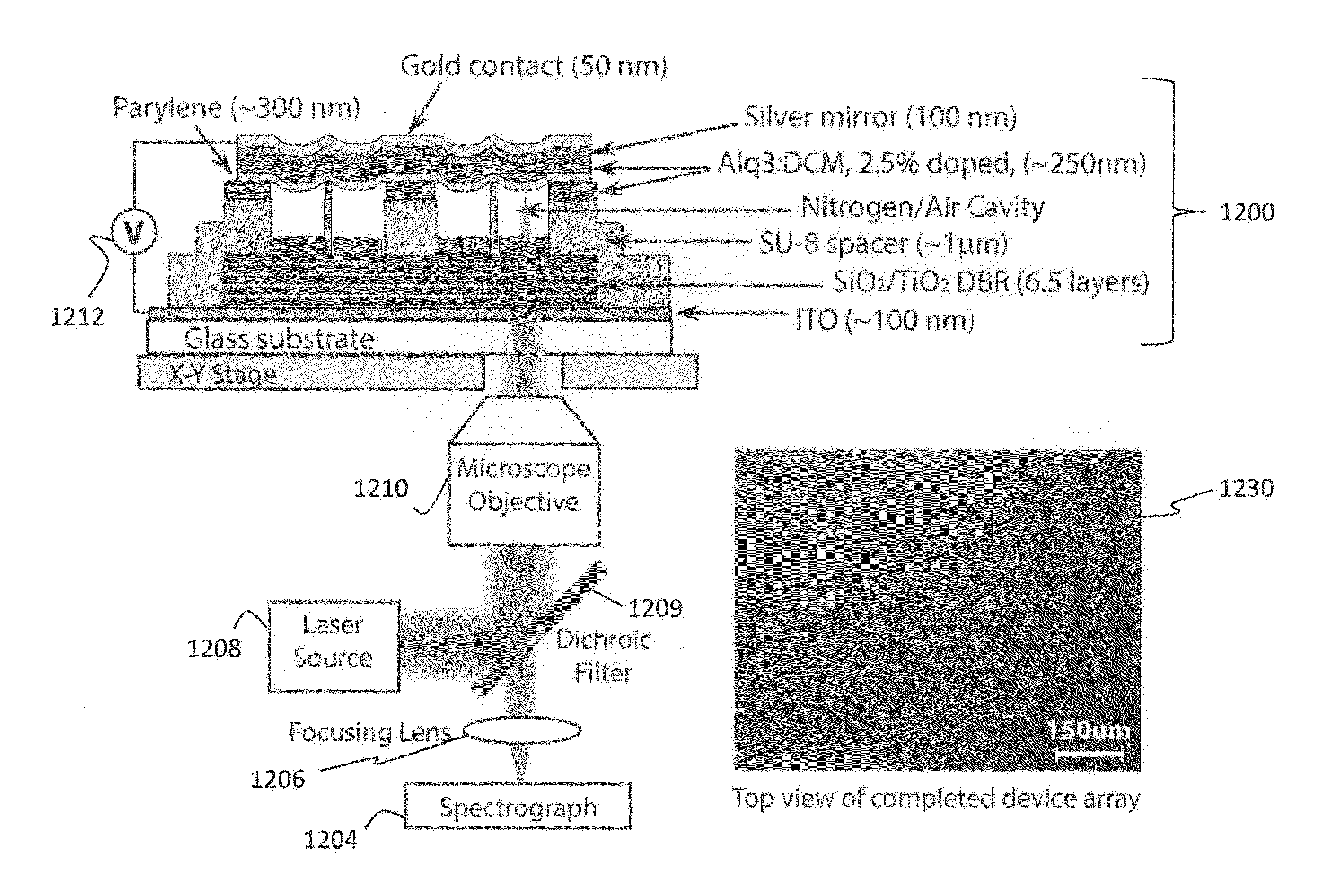
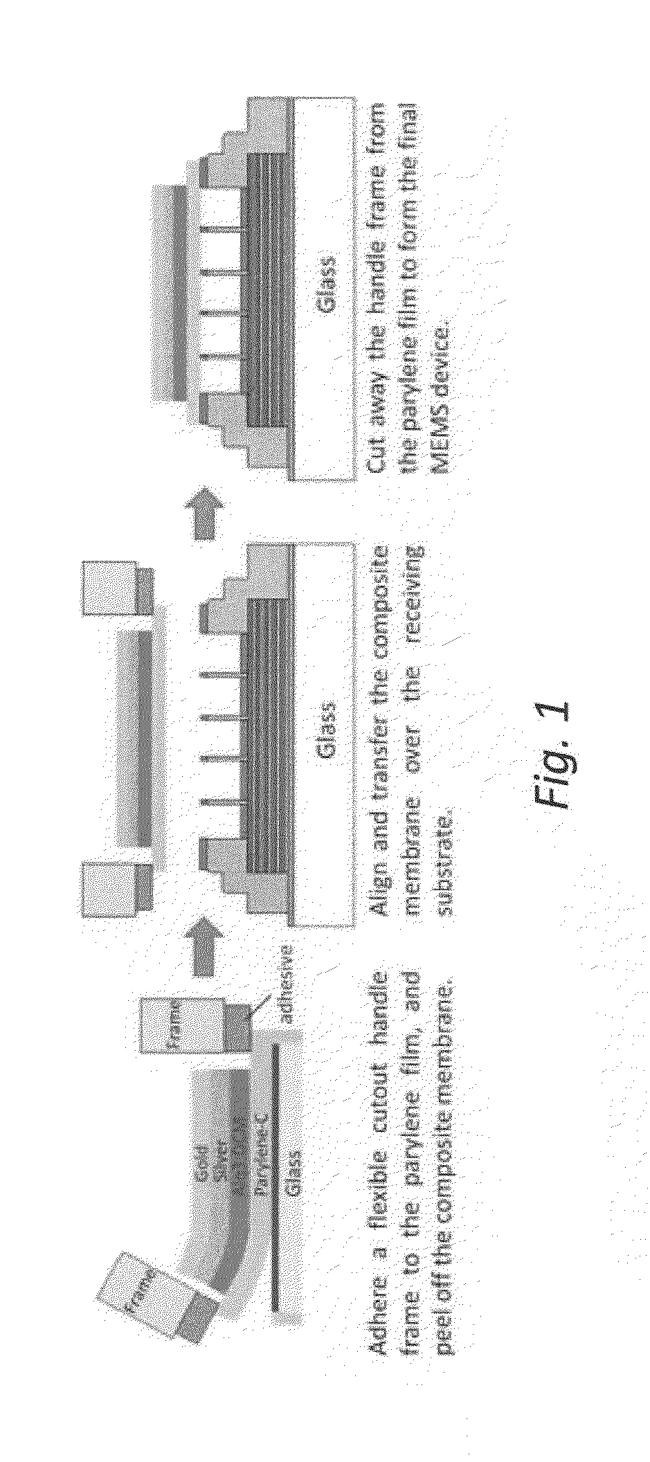
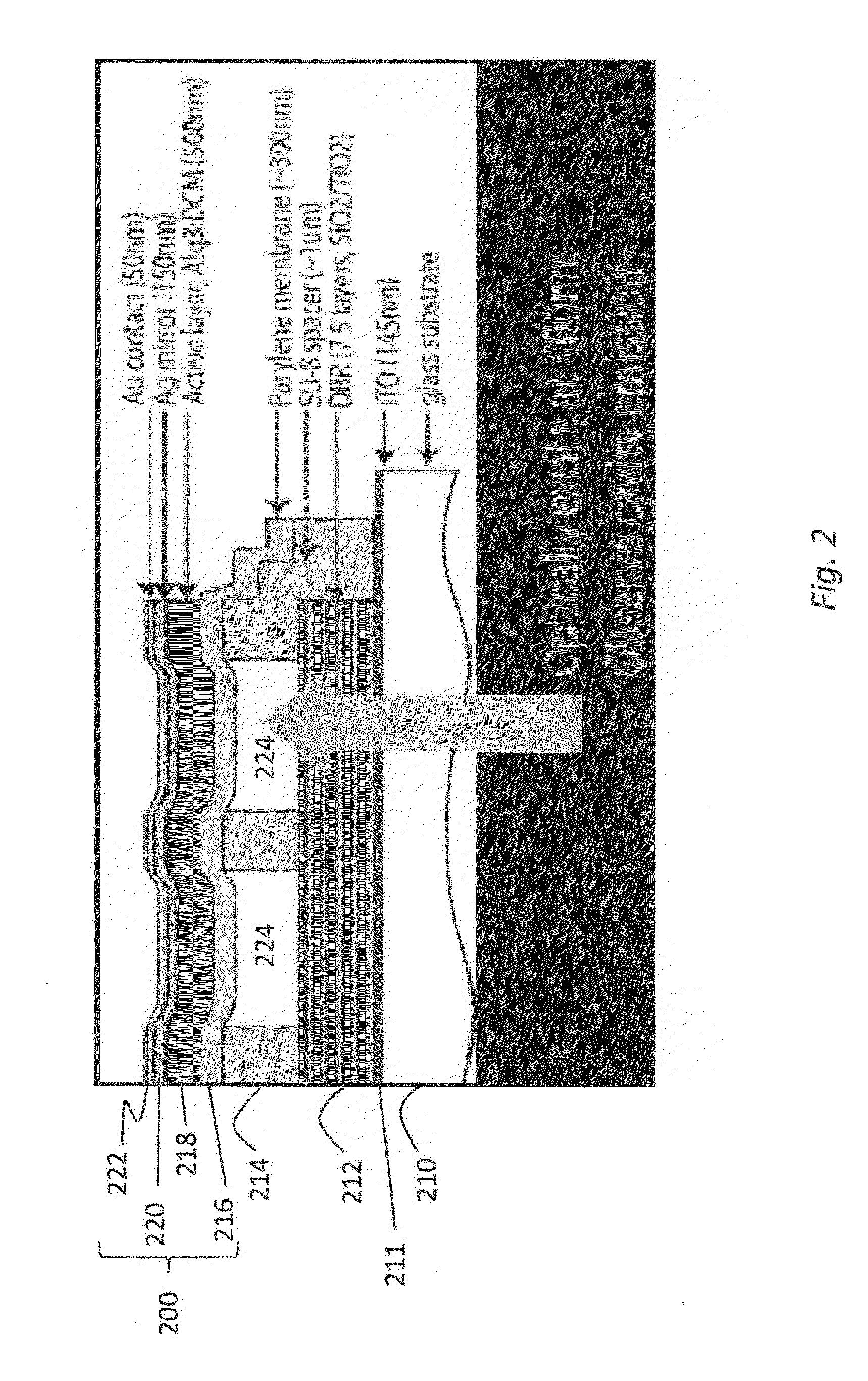
[0032]The disclosed embodiments are generally directed to a solvent-free, room-temperature method for transferring very thin unsupported functional films along with several novel MEMS and optoelectronic devices that can be fabricated using such suspended micron- and submicron-thick composite membranes. In one application, poly-para-xylylenes (Parylenes) are used as very thin unsupported functional films.

[0033]In one embodiment, the disclosure relates to a solvent-free room-temperature method for transferring very thin unsupported functional films along with novel MEMS and optoelectronic devices fabricated using the disclosed suspended micron- and submicron-thick composite membranes. The solvent-free release and transfer technique for thin membranes may be enabled by using a micron- or sub-micron-thick vapor-deposited polymer, parylene. The chemically robust parylene film can be compatible with both vapor- and solution-based deposition methods useful for the fabrication of composite ...


PUM

PropertyMeasurementUnit
thicknessaaaaaaaaaa
voltageaaaaaaaaaa
thicknessaaaaaaaaaa

Abstract

The disclosure relates to method and apparatus for micro-contact printing of micro-electromechanical systems (“MEMS”) in a solvent-free environment. The disclosed embodiments enable forming a composite membrane over a parylene layer and transferring the composite structure to a receiving structure to form one or more microcavities covered by the composite membrane. The parylene film may have a thickness in the range of about 100 nm-2 microns; 100 nm-1 micron, 200-300 nm, 300-500 nm, 500 nm to 1 micron and 1-30 microns. Next, one or more secondary layers are formed over the parylene to create a composite membrane. The composite membrane may have a thickness of about 100 nm to 700 nm to several microns. The composite membrane's deflection in response to external forces can be measured to provide a contact-less detector. Conversely, the composite membrane may be actuated using an external bias to cause deflection commensurate with the applied bias. Applications of the disclosed embodiments include tunable lasers, microphones, microspeakers, remotely-activated contact-less pressure sensors and the like.

Description

[0001]The application claims the filing-date priority of Provisional Application No. 61 / 903,507 (filed Nov. 13, 2013) and is a continuation-in-part (CIP) of application Ser. No. 13 / 844,270, filed Mar. 15, 2013, which claimed priority to Provisional Application Ser. No. 61 / 696,041, filed Aug. 31, 2012; the instant application is also a continuation-in-part (CIP) of application Ser. No. 13 / 604,613, filed Sep. 5, 2012 (which claims priority to Provisional Application No. 61 / 528,148, filed Aug. 27, 2011); and application Ser. No. 12 / 636,757 (now U.S. Pat. No. 8,739,390), filed Dec. 13, 2009 (which claims priority to Provisional Application Ser. No. 61 / 138,014, filed Dec. 16, 2008); the instant application is also a continuation-in-part (CIP) of application Ser. No. 12 / 903,149, filed Oct. 12, 2010 (which claims priority to Provisional Application No. 61 / 251,255, filed Oct. 13, 2009). The disclosure of each of these applications are incorporated herein in its entirety.BACKGROUND[0002]1. F...

Claims


Application Information

Patent Timeline
Patent Type & Authority Applications(United States)
IPC IPC(8): H01S3/106H01S3/0941H01S3/07G02B26/00H01S3/16H01S3/13H01S3/105H01S3/0933H01S3/08
CPCH01S3/106H01S3/0933H01S3/0941H01S3/07G02B26/001H01S3/16H01S3/1693H01S3/1305H01S3/1053H01S3/08059B81C1/00158B81C1/00634B81B2201/042B81C2201/0194G01L11/02G01L9/0005G01L9/0072H01L29/84B81B2201/02G01L1/24H01S3/094
Inventor BULOVIC, VLADIMIRLANG, JEFFREY HASTINGSMURARKA, APOORVAWANG, ANNIE I-JENCHANG, WENDI
Owner MASSACHUSETTS INST OF TECH
Why Eureka
Try Eureka