Plasmonic optical waveguide using plasmonic coupling between nano-aperture and nano-particle

a plasmonic optical waveguide and nano-aperture technology, applied in the field of plasmonic optical waveguides, can solve the problems of difficult to obtain a few tens of nanometers, which is needed for a microscope, a semiconductor or the like, and the intensity of the output beam is low, and achieves a very small collected light compared with the incident light, and achieves a high optical amplification rate. , the effect of reducing the size of the collected ligh

Active Publication Date: 2015-11-19
IND ACADEMIC CORP FOUND YONSEI UNIV
View PDF1 Cites 2 Cited by
  • Summary
  • Abstract
  • Description
  • Claims
  • Application Information

AI Technical Summary

Problems solved by technology

However, although it is possible to secure an NA larger than one by using an immersion material, a resolution of a few tens of nanometers, which is needed for a microscope, a semiconductor or the like, is difficult to obtain since the refractive index is limited.
However, since the amount of the transmitted light is limited, there is a problem in that intensity of the output beam is low.
However, since the conventional optical amplification technique based on the nano-opening accomplishes the optical amplification through surface plasmon resonance by using only a peculiar geometric shape of the nano-opening, there is a limit in obtaining an output light having a high optical amplification rate and a very small collected light compared with the incident light.
Accordingly, it is disadvantageous in that it is difficult to obtain high-intensity and high-density output optical energy needed for the optical information storage device, the near field scanning optical microscopy (NSOM), the lithography and the like.
In addition, since the nano-opening should approach a sample (medium) at a gap of a few tens of nanometers to demonstrate performance of the nano-opening, it is disadvantageous in that the nano-opening is exposed to damage and contamination.
Accordingly, it is disadvantageous in that if a dielectric layer is arranged on the bottom surface of the nano-opening, performance of the nano-opening is seriously lowered, and if the dielectric layer is not arranged, the nano-opening is highly probable to be damaged and contaminated since it is exposed to use environments as is.
Although a method of primarily amplifying light at the nano-opening and secondarily re-amplifying the light between metal nano-particles using a multi-surface plasmon resonance effect has been introduced to solve the problems, there is a problem in that since this method is sensitive to arrangement of nano-particles, light can be emitted when an error of a few nanometers occur at the gap between the particles.

Method used


Image

  • Plasmonic optical waveguide using plasmonic coupling between nano-aperture and nano-particle
  • Plasmonic optical waveguide using plasmonic coupling between nano-aperture and nano-particle
  • Plasmonic optical waveguide using plasmonic coupling between nano-aperture and nano-particle

Examples


Embodiment Construction

[0032]Although the preferred embodiments of the present invention will be hereafter described in detail with reference to the accompanying drawings, the scope of the present invention is not limited thereto. Detailed description will be omitted for publicized configurations, and in addition, if a configuration may make the spirit of the present invention unclear, detailed description thereof will be omitted.

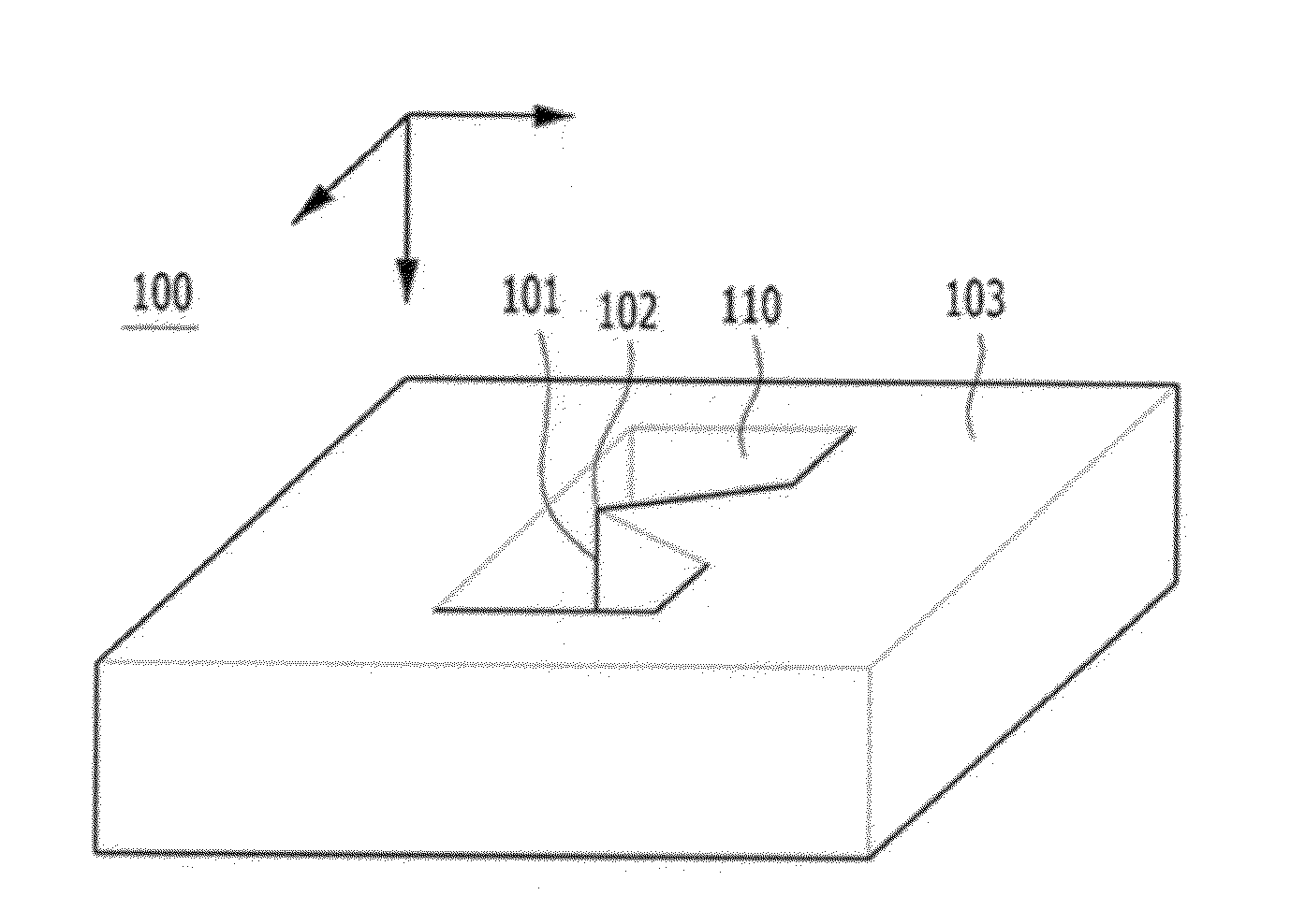
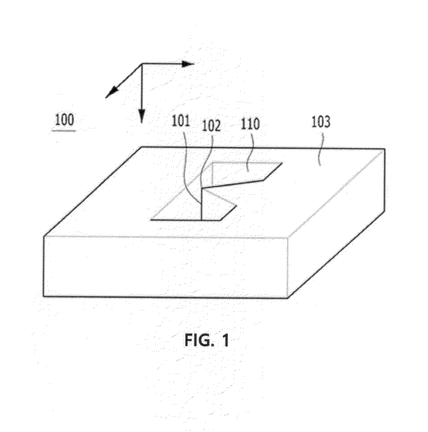
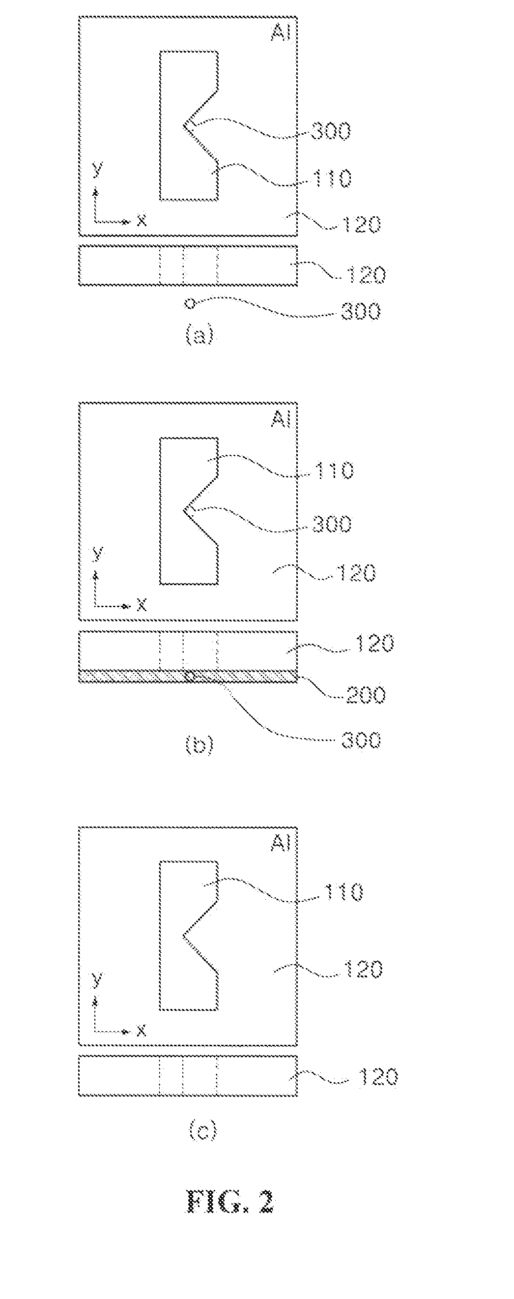
[0033]A plasmonic optical waveguide of the present invention is a module capable of amplifying an optical signal, which is a kind of electromagnetic wave, to have a high amplification rate compared with incident light and may be configured to include a nano-aperture 100 formed with an opening 110 of a nano-scale and a metal nano-particle. In addition, it may be configured to additionally include a dielectric layer 200 combined at the outlet side of the nano-aperture 100.

[0034]The nano-aperture 100 may be a kind of optical element. The nano-aperture 100 may form a light spot by us...


PUM


Abstract

The present invention relates to a plasmonic optical waveguide using plasmonic coupling between a nano-aperture and a nano-particle. The plasmonic optical waveguide includes the nano-aperture formed with an opening of a nano-scale through which light enters; and a single metal nano-particle arranged at the focal point of the nano-aperture to generate plasmon coupling in association with the light output from the nano-aperture. The plasmonic optical waveguide has an effect of forming a small and strong high-intensity high-density light spot of a sub-wavelength size, in which an amplification rate is increased at the output surface of the nano-particle more than a few hundred times compared with the incident light, since the light is transmitted by plasmon coupling generated between the nano-aperture and the nano-particle.

Description

BACKGROUND OF THE INVENTION[0001]1. Field of the Invention[0002]The present invention relates to a plasmonic optical waveguide using plasmonic coupling between a nano-aperture and a nano-particle, and more specifically, to a plasmonic optical waveguide which can amplify light output from a nano-aperture by transmitting the light without loss through a nano-particle using plasmonic coupling.[0003]2. Background of the Related Art[0004]High-intensity light of a small size is needed in many fields such as an optical information storage device, a near field scanning optical microscopy (NSOM), lithography and the like. A general method used for generating the small and strong high-intensity light is refracting incident light using a lens. At this point, the minimum size of an output beam cannot be smaller than a diffraction limit Δ of light as shown in the following equation.Δ=λ2nsin(θ)=λ2NA[0005]In the above equation, Δ denotes a diffraction limit, λ denotes wavelength of light, n denote...

Claims


Application Information

Patent Timeline
Patent Type & Authority Applications(United States)
IPC IPC(8): G02B6/122G02B6/10H01S3/16H01S3/063
CPCG02B6/1226H01S3/063Y10S977/773H01S3/169B82Y20/00G02B6/107
Inventor PARK, NO CHEOLLEE, WON SUPKIM, DO HYUNGMOON, HYUNGBAECHOI, GUK JONGJEON, SUNGBINLIM, GEON
Owner IND ACADEMIC CORP FOUND YONSEI UNIV
Why Eureka
Try Eureka