Compound for organic electric element, organic electric element comprising the same and electronic device thereof

a technology of organic electric elements and organic electric elements, which is applied in the field of organic electric element compounds, can solve the problems of reducing the efficiency of corresponding elements, reducing the luminescence efficiency, and shifting the maximum luminescence wavelength to a longer wavelength, so as to improve the luminous efficiency, low driving voltage, and the effect of improving the color purity and luminous efficiency

Active Publication Date: 2015-12-03
DUK SAN NEOLUX +1
View PDF1 Cites 7 Cited by
  • Summary
  • Abstract
  • Description
  • Claims
  • Application Information

AI Technical Summary

Benefits of technology

[0015]By using the compound according to embodiments of the present invention, an organic electric element according to one or more embodiments of the present invention not only has low driving voltage and high heat-resistant and, but can also be significantly improved in color purity, luminous efficiency, and life span.

Problems solved by technology

Meanwhile, when only one material is used as a light emitting material, there occur problems of shift of a maximum luminescence wavelength to a longer wavelength due to intermolecular interactions and lowering of the efficiency of a corresponding element due to a deterioration in color purity or a reduction in luminous efficiency.
Currently, the power consumption is required more and more as size of display becomes larger and larger in the portable display market.
The most problematic issues in an organic electric element are life span and efficiency, and the situation is such that this life span or efficiency issue must be solved as displays become larger and larger.
However, efficiency cannot be maximized only by simply improving the organic material layer.
However, such a stable and efficient organic material layer material for an organic electric element has not yet been fully developed.

Method used


Image

  • Compound for organic electric element, organic electric element comprising the same and electronic device thereof
  • Compound for organic electric element, organic electric element comprising the same and electronic device thereof
  • Compound for organic electric element, organic electric element comprising the same and electronic device thereof

Examples


synthesis example

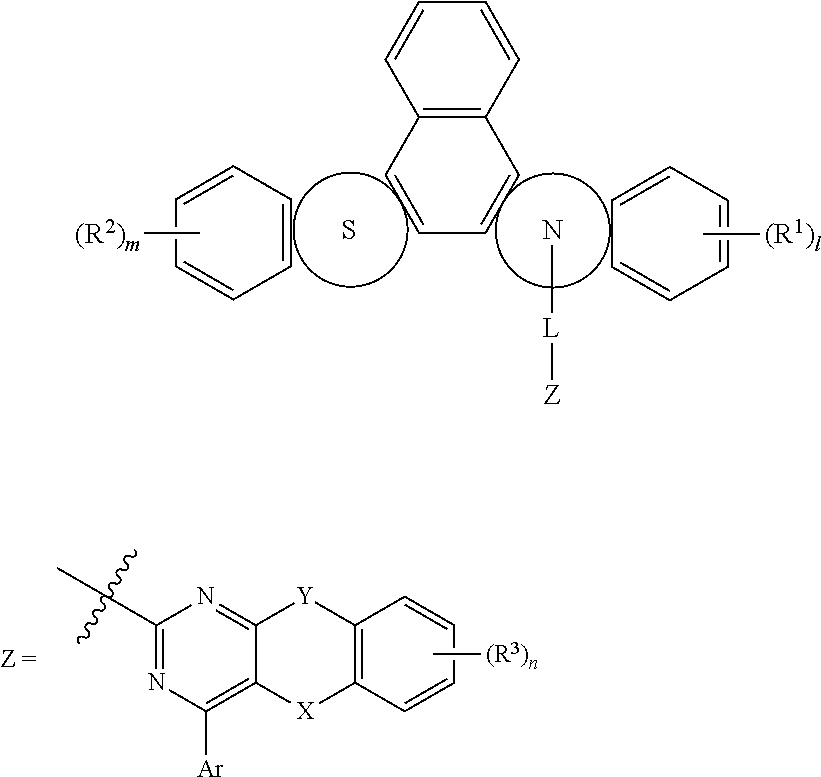
[0084]The final product according to the present invention can be synthesized by reaction between Sub 1 and Sub 2 as illustrated in, but not limited to, the following Reaction Scheme 1.

I. Synthesis of Sub 1

[0085]Sub 1 of Reaction Scheme 1 can be synthesized according to, but not limited to, the following Reaction Scheme 2.

[0086]Synthesis Examples of the compounds of Sub 1 will be described in detail.

1. Sub 1-1 Synthesis

[0087]

(1) 1-1-C1 Synthesis

[0088]To a solution of the starting material 5-bromobenzo[b]naphtha[1,2-d]thiophene (50 g, 0.16 mol), bis(pinacolato)diboron (48.65 g, 0.19 mol), KOAc (47 g, 0.48 mol) and PdCl2(dppf) (5.21 g, 4 mol %) were dissolved in DMF, followed by reflux at 100° C. for 12 hours. Upon completion of the reaction, the temperature of the reaction product was lowered to room temperature, the reaction product was extracted with CH2Cl2, and was washed with water. The extracted organic layer was dried with MgSO4 and concentrated, and then the produced organic m...


PUM

PropertyMeasurementUnit
thicknessaaaaaaaaaa
thicknessaaaaaaaaaa
thicknessaaaaaaaaaa

Abstract

A compound represented by Formula 1. An organic electric element includes a first electrode, a second electrode, and an organic material layer between the first electrode and the second electrode. The organic material layer includes the compound represented by Formula 1. When the organic electric element includes the compound in the organic material layer, driving voltage, luminous efficiency, color purity, stability, and life span can be improved.

Description

CROSS-REFERENCE TO RELATED APPLICATION[0001]This application claims priority from and the benefit under 35 U.S.C. §119(a) of Korean Patent Application No. 10-2014-0064229, filed on May 28, 2014, the contents of which are hereby incorporated by reference for all purposes as if fully set forth herein.BACKGROUND[0002]1. Technical Field[0003]The present invention relates to a compound for an organic electric element, an organic electric element using the same, and an electronic device thereof[0004]2. Background Art[0005]In general, an organic light emitting phenomenon refers to a phenomenon in which electric energy is converted into light energy of an organic material. An organic electric element utilizing the organic light emitting phenomenon usually has a structure including an anode, a cathode, and an organic material layer interposed therebetween. Here, in many cases, the organic material layer may have a multilayered structure including multiple layers made of different materials i...

Claims


Application Information

Patent Timeline
Patent Type & Authority Applications(United States)
IPC IPC(8): H01L51/00H01L27/30H01L27/32H01L27/28C07D495/04C09K11/06H05B44/00
CPCH01L51/0071C07D495/04C09K11/06H01L27/3244H01L27/283H01L27/301H01L51/0067H01L51/0052H01L51/0072H01L51/0073H01L51/0074H01L51/5206C07D519/00H10K85/6576H10K85/6574H10K85/657H10K85/6572H10K50/11C09K2211/1029C09K2211/1037C09K2211/1048C09K2211/1051C09K2211/1092C09K2211/185C07D491/04Y02E10/549H10K71/13H10K71/135H10K85/615H10K85/654H10K10/46H10K30/00H10K2101/10C09K2211/1088H10K19/10H10K39/10H10K59/12H10K50/81H10K50/82C09K2211/1007C09K2211/1011C09K2211/1044
Inventor PARK, JUNGHWANKIM, WONSAMBYUN, JIHUNPARK, JEONGKEUNJUNG, HWASOONCHOI, YEONHEEKIM, SEOKHYUNLEE, KWANHEEKIM, MIKYUNG
Owner DUK SAN NEOLUX
Why Eureka
Try Eureka