

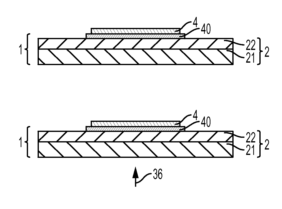
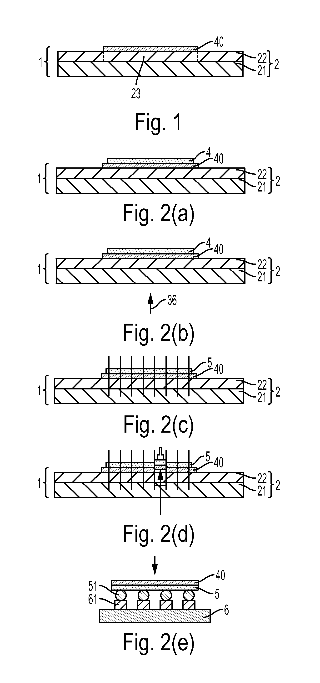
Dicing-tape integrated film for backside of semiconductor and method of manufacturing semiconductor device
a technology of integrated film and semiconductor, which is applied in the direction of transportation and packaging, synthetic resin layered products, chemistry apparatus and processes, etc., can solve the problems of laser marking cannot be preferably performed, the coloring agent in the film for the backside of a flip-chip semiconductor is transferred, etc., and achieves high polarity, high polarity, and suppression of the transfer of coloring agent onto the pressure-sensitive layer
- Summary
- Abstract
- Description
- Claims
- Application Information
AI Technical Summary
Benefits of technology
Problems solved by technology
Method used
Image

Examples
example 1
[0152]
[0153]To 100 parts of an acrylic ester based polymer (Paracron W-197CM, SP value 12, manufactured by Negami Chemical Industrial Co., Ltd.) having ethylacrylate as a main component, 113 parts of an epoxy resin (Epicoat 1004, manufactured by Japan Epoxy Resins Co., Ltd.), 121 parts of a phenol resin (MEH-7851H, manufactured by Meiwa Plastic Industries, Ltd.), 246 parts of spherical silica (SO-25R, manufactured by ADMATECHS Co., Ltd.), and 5 parts of dye (OIL BLACK SOM-L-0543, manufactured by Orient Chemical Industries Co., Ltd.) were dissolved in methyethylketone to prepare an adhesive composition solution having a concentration of solid content of 23.6% by weight.
[0154]This adhesive composition solution was applied onto a release-treated film consisting of a silicon release-treated polyethyleneterephthalate film having a thickness of 50 μm as a release liner, and dried at 130° C. for 2 minutes to form a film A for the backside of a semiconductor having a thickness of 20 μm.
[015...
example 2
[0163]
[0164]The film B for the backside of a semiconductor according to Example 2 was produced in the same way as Example 1 except “ORIPACS B-1” (manufactured by Orient Chemical Industries Co., Ltd.) was used as a coloring agent instead of “OIL BLACK SOM-L-0543” (manufactured by Orient Chemical Industries Co., Ltd.) “ORIPACS B-1” is a dye having a chromium complex.
[0165]
[0166]The film B for the backside of a semiconductor was pasted onto the pressure-sensitive adhesive layer of the dicing tape A that was produced in Example 1 using a hand roller to produce the dicing-tape integrated film B for the backside of a semiconductor according to Example 2.
example 3
[0167]
[0168]The film C for the backside of a semiconductor according to Example 3 was produced in the same way as Example 1 except “SDO-7” (manufactured by Orient Chemical Industries Co., Ltd.) was used as a coloring agent instead of “OIL BLACK SOM-L-0543” (manufactured by Orient Chemical Industries Co., Ltd.) “SDO-7” is a dye having an anthraquinone skeleton.
[0169]
[0170]The film C for the backside of a semiconductor was pasted onto the pressure-sensitive adhesive layer of the dicing tape A that was produced in Example 1 using a hand roller to produce the dicing-tape integrated film C for the backside of a semiconductor according to Example 3.
PUM
| Property | Measurement | Unit |
|---|---|---|
| solubility | aaaaa | aaaaa |
| surface free energy E2 | aaaaa | aaaaa |
| solubility | aaaaa | aaaaa |
Abstract
Description
Claims
Application Information