Laminar structure of semiconductor and manufacturing method thereof

a semiconductor and lattice technology, applied in semiconductor devices, semiconductor/solid-state device details, electrical devices, etc., can solve the problems of reducing component yield, higher cost, and reducing lattice mismatch (up to 34% of the difference in thermal expansion coefficient), so as to reduce the stress effect, avoid bending, and improve yield

Active Publication Date: 2015-12-10
GLOBALWAFERS CO LTD
View PDF5 Cites 7 Cited by
  • Summary
  • Abstract
  • Description
  • Claims
  • Application Information

AI Technical Summary

Benefits of technology

[0009]The present invention is directed to providing a laminar structure of semiconductor provided with a protective layer on the rear side of the substrate so as to reduce the stress effect between the epitaxial layer and the substrate to avoid bending and crack phenomenon, and further achieve improved yield and saved cost.

Problems solved by technology

Bending or crack due to excessive tensile stress may occur during the cooling process after completion of GaN epitaxial film growth and result in reduced component yield.
Adopting a sapphire (Al2O3) substrate may have the same problem (16% lattice mismatch and 34% differences in thermal expansion coefficient) with higher cost.
However, the cost of SiC is too high for commercial development.
However, the buffer layer must be provided with good lattice structure in order to grow the epitaxial layer with good quality; therefore, it still needs high-temperature crystal growth process, which is complicated and expensive.

Method used


Image

  • Laminar structure of semiconductor and manufacturing method thereof
  • Laminar structure of semiconductor and manufacturing method thereof
  • Laminar structure of semiconductor and manufacturing method thereof

Examples


Embodiment Construction

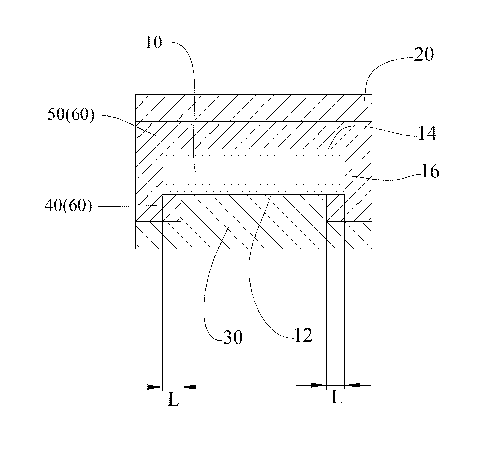
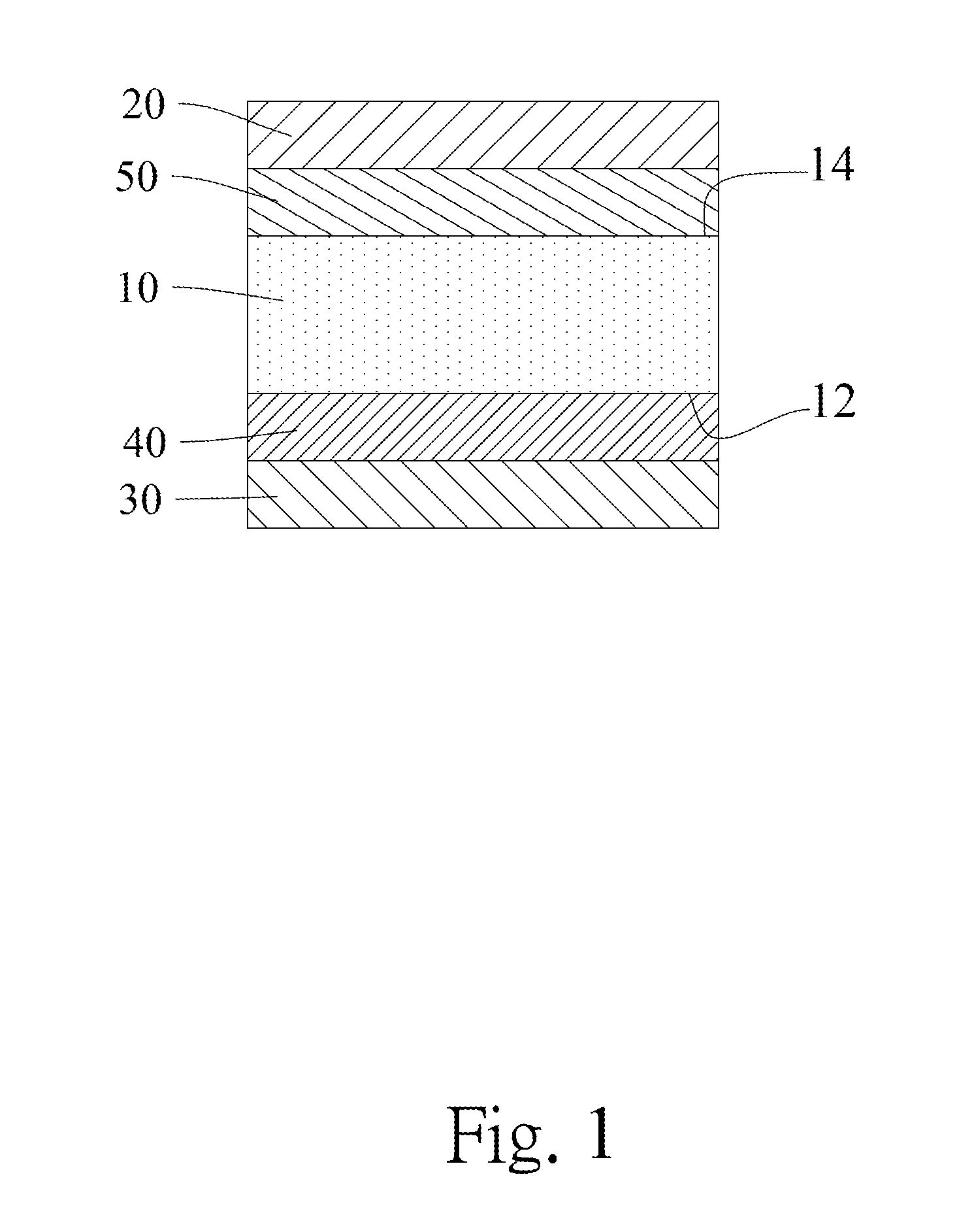
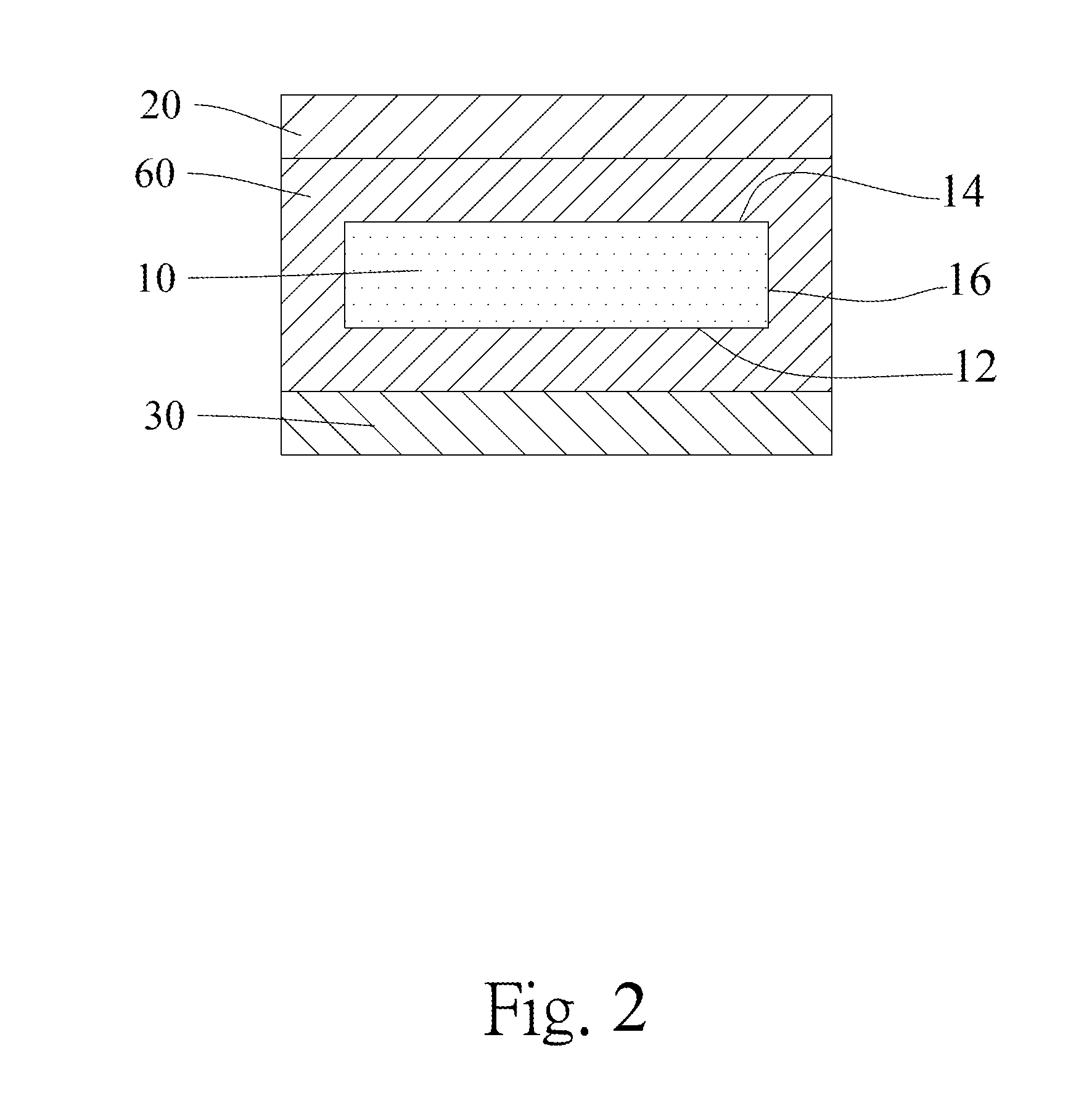
[0020]Refer to FIG. 1, which is a schematic diagram illustrating a laminar structure of semiconductor according to one embodiment of the present invention. The laminar structure of semiconductor includes a substrate 10, an epitaxial layer 20, a protective layer 30, a first layer 40 and a second layer 50. The epitaxial layer 20 is arranged above the substrate 10. The protective layer 30 is arranged below the substrate 10, wherein the thermal expansion coefficients of the epitaxial layer 20 and the protective layer 30 are simultaneously greater than or less than that of the substrate 10. The first layer 40 is arranged on a lower surface 12 of the substrate 10 and between the substrate 10 and the protective layer 30, wherein a band gap of the first layer 40 is greater than 3 eV; and / or the second layer 50 is arranged on an upper surface 14 of the substrate 10 and between the substrate 10 and the epitaxial layer 20, wherein a band gap of the second layer 50 is greater than 3 eV. Further...


PUM


Abstract

A laminar structure of semiconductors comprises a substrate, an epitaxial layer, a protective layer, a first layer and a second layer. The epitaxial layer is arranged above the substrate and the protective layer is arranged below the substrate. Thermal expansion coefficients of the epitaxial layer and the protective layer are simultaneously greater than or less than that of the substrate. The first layer is arranged between the substrate and the protective layer; and the second layer is arranged between the substrate and the epitaxial layer, wherein the band gap of the first layer and the second layer are both greater than 3 eV. By a protective layer arranged below the substrate, stress generated between the substrate and the epitaxial layer can be reduced to prevent occurrence of bending or crack. Therefore, yield can be promoted and costs can be reduced. A manufacturing method thereof is also herein provided.

Description

BACKGROUND OF THE INVENTION[0001]1. Field of the Invention[0002]The present invention relates to a laminar structure of semiconductor, in particular to a laminar structure of semiconductor that is applied to a semiconductor component.[0003]2. Description of the Prior Art[0004]Among semiconductor materials, gallium nitride (GaN) is provided with good electrical conductivity, thermal conductivity and thermal stability, and thus can be used as high-power components. In addition, due to the wide band-gap, GaN is capable of emitting at the green to violet wavelength and is also suitable as a full-color light-emitting element. However, the substrate, such as silicon substrate, for epitaxial growth of GaN has huge differences in lattice constant and thermal expansion coefficient from GaN, namely 17% and 46%, respectively; therefore, there exists considerable stress field between these two. Bending or crack due to excessive tensile stress may occur during the cooling process after completio...

Claims


Application Information

Patent Timeline
Patent Type & Authority Applications(United States)
IPC IPC(8): H01L23/00H01L21/768H01L21/02H01L29/20H01L23/532
CPCH01L23/562H01L29/2003H01L21/76841H01L23/53271H01L21/0254H01L23/53209H01L21/02381H01L21/02433H01L21/02458H01L21/02488H01L29/205H01L2924/0002
Inventor HSU, WEN-CHINGKO, CHIA-WENLUO, CHIOU-MEI
Owner GLOBALWAFERS CO LTD
Why Eureka
Try Eureka