Graphene transistor optical detector based on metamaterial structure and application thereof

a graphene transistor and optical detector technology, applied in the direction of radio frequency controlled devices, semiconductor devices, electrical apparatuses, etc., can solve the problem of less than 10 layers of graphene light absorption efficiency, which is far lower than the efficiency of other bulk materials or quantum well structures, and achieves improved detector sensitivity.

Active Publication Date: 2015-12-10
SUZHOU INST OF NANO TECH & NANO BIONICS CHINESE ACEDEMY OF SCI
View PDF5 Cites 39 Cited by
  • Summary
  • Abstract
  • Description
  • Claims
  • Application Information

AI Technical Summary

Benefits of technology

[0017]by integrating the graphene layer in the metamaterial structure having an approximately complete absorption characteristic, the absorption of graphene to light, i.e., the sensitivity of the detector, is improved;

Problems solved by technology

However, the effective absorption of single-layer or multi-layer (less than 10 layers) graphene to light is far lower than the efficiency of other bulk materials or quantum well structures.
Although the above technologies all show a certain degree of enhancement of light absorption of graphene by microcavity, plasmon or other effects, more effective technical solutions need to be further explored in the art due to the complexity of technical processes and the limitations to the performance enhancement.

Method used


Image

  • Graphene transistor optical detector based on metamaterial structure and application thereof
  • Graphene transistor optical detector based on metamaterial structure and application thereof
  • Graphene transistor optical detector based on metamaterial structure and application thereof

Examples


embodiment 1

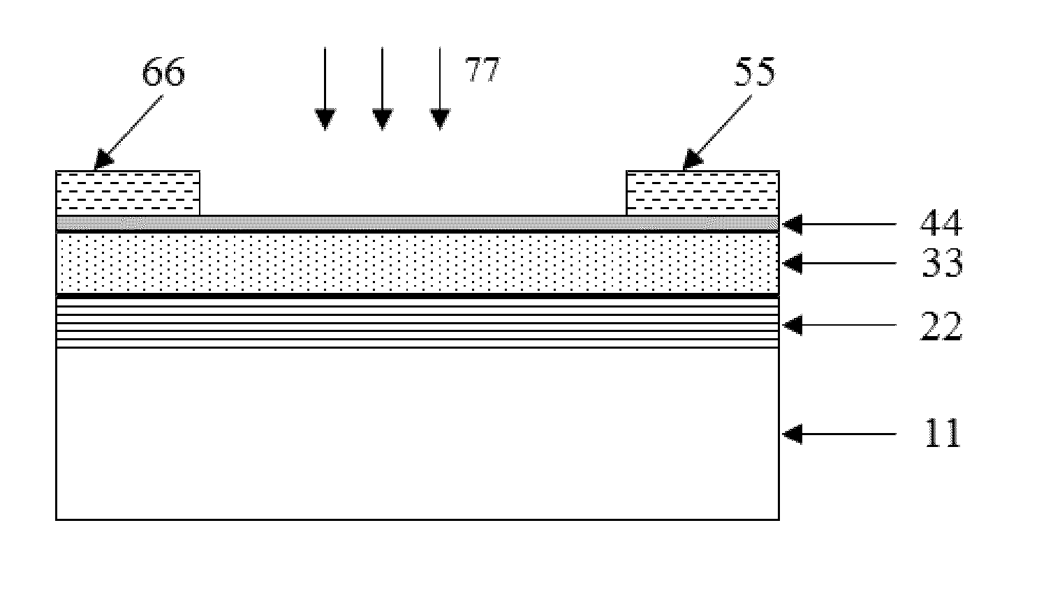
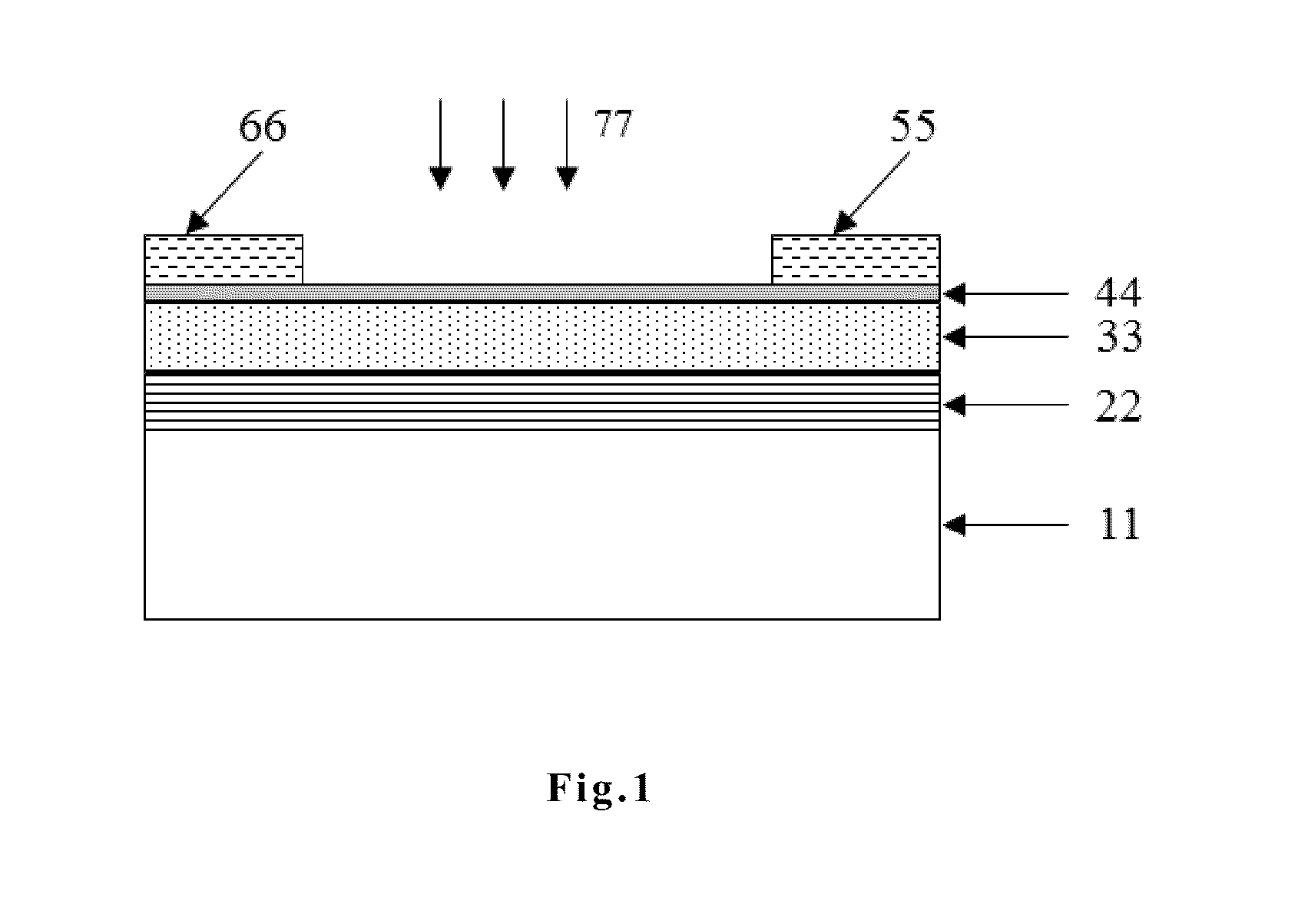
[0053]Referring to FIG. 1, a longitudinally sectional view of the graphene transistor optical detector based on a metamaterial structure provided in this embodiment is shown. The detector includes a substrate 11, a gate metal layer 22, a gate medium layer 33, a graphene layer 44 and a source 55 and drain 66 metal layer. In FIG. 1, the incident light is indicated by arrow 77. In this embodiment, the gate metal layer 22 forms a reflective layer of the metamaterial, and the source 55 and drain 66 metal layer forms a surface impedance matching layer of the metamaterial. By optimizing the gate medium layer 33 and a periodic structure of a source 55 and a drain 66, approximately complete absorption in a preset waveband may be obtained. Meanwhile, the gate metal layer 22 may be used as a gate of a transistor for regulating the band gap of the graphene layer 44 and forming a carrier conductive channel, thereby realizing photoelectrical conversion. In this embodiment, by integrating the grap...

embodiment 2

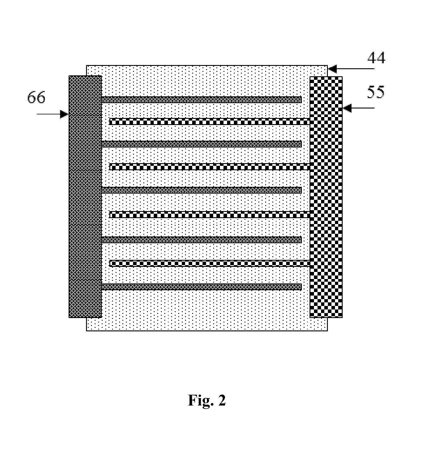
[0055]The longitudinally sectional view of this embodiment may refer to FIG. 1, and the top view thereof may refer to FIG. 3. A difference between this embodiment and Embodiment 1 mainly lies in that, the source 55 and the drain 66 in this embodiment form a two-dimensional structure, and the surface impedance matching layer of the resulting metamaterial may result in near-zero reflection to incident light in different polarization directions, so that the photoelectrical efficiency of the detector is further improved.

[0056]In this embodiment, the following specific materials and structures may be selected, wherein the gate material layer 22 is made of gold and has a thickness of at last 50 nm; the gate medium layer 33 is made of aluminum oxide (Al2O3) and has a thickness of 10 nm; the source 55 and the drain 66 are both made of gold and each have a thickness of 70 nm; and, the periodic micro / nanostructure formed by a partial structure of the source and drain metal layer has a side le...

embodiment 3

[0057]Referring to FIG. 4, a top view of graphene transistor optical detectors based on metamaterial structures during imaging application according to this embodiment is shown, where A, B, C and D denote graphene transistor detectors working in different preset wavebands, respectively, and the structure of each of these graphene transistor optical detectors may be any one of Embodiment 1 and Embodiment 2. By integrating the detectors A, B, C and D into a pixel I and periodically arranging this pixel to form a whole image sensor, multi-waveband imaging may be realized. For example, A and D are graphene transistor optical detectors working in blue and red wavebands while B and C are graphene transistor optical detectors working in a green waveband, then, an image sensor similar to a RGB (red, green, blue) color image sensor is formed. By optimizing various integration solutions of the graphene transistor detectors working in different wavebands, a multi-waveband super camera may be o...


PUM


Abstract

A graphene transistor optical detector based on a metamaterial structure and an application thereof. The optical detector includes a substrate, a gate metal layer, a gate medium layer, a graphene layer, a source and drain metal layer successively arranged from bottom to top, wherein a local region of at least the source and drain metal layer has a periodic micro/nanostructure, the periodic micro/nanostructure being matched with the gate metal layer and the gate medium layer to form a metamaterial structure having a complete absorption characteristic. By changing the refractive index, thickness or the like of material for the periodic micro/nanostructure and the gate medium layer, a light absorption frequency band of the metamaterial structure can be regulated. The optical detector provided by the present invention has higher flexibility and narrow-band response, and can work under visible light to infrared even longer wavebands by selecting different metamaterial structures.

Description

TECHNICAL FIELD OF THE INVENTION[0001]The present invention relates to an optical detection device, in particular to an absorption-enhanced graphene field effect transistor optical detector based on a micro / nanostructure and an imaging application thereof.BACKGROUND OF THE INVENTION[0002]Graphene is a two-dimensional layered material structure of carbon. The single-layer graphite has a thickness of about 0.35 nm and has outstanding electrical, optical and mechanical characteristics. Graphite of not more than ten layers is regarded as graphene. Since the successful development of single-layer graphene in 2004, graphene has drawn great attention. Due to its Dirac-Fermi property, linear energy band structure and the highest carrier mobility (200000 cm2 v−1 s-1) among the materials that have been discovered so far, graphene has been widely applied in the field of high-frequency nano-electronic devices. Meanwhile, graphene has remarkable optical characteristics and a flat absorption band...

Claims


Application Information

Patent Timeline
Patent Type & Authority Applications(United States)
IPC IPC(8): H01L31/113H01L29/423H01L29/16H01L29/08H01L27/146H01L31/028
CPCH01L31/1136H01L27/146H01L29/42372H01L29/1606H01L29/0847H01L31/028H01L31/02162Y02E10/547
Inventor CHEN, QINSONG, SHICHAO
Owner SUZHOU INST OF NANO TECH & NANO BIONICS CHINESE ACEDEMY OF SCI
Why Eureka
Try Eureka