Microelectronic assemblies with integrated circuits and interposers with cavities, and methods of manufacture

Active Publication Date: 2016-01-14
INVENSAS CORP
View PDF0 Cites 17 Cited by
  • Summary
  • Abstract
  • Description
  • Claims
  • Application Information

AI Technical Summary

Benefits of technology

[0009]Some manufacturing techniques described below reduce the assembly size and improve the mechanical strength and heat-dissipation capabilities of IC assemblies and intermediate structures. For example, in some embodiments, the structure of FIG. 1 is modified by providing the interposer 120.2 with a cavity on the bottom (shown as cavity 202.2 in FIG. 2), and the die 110.2 can be placed in the cavity; or the die can be placed in a cavity 202.1 in the top surface of interposer 120.1; in FIG. 2, the die enters both cavities. Therefore, the interposers 120.1 and 120.2 can be brought closer together, shortening the studs 154 interconnecting the two interposers. The assembly size is reduced, and so is the amount of encapsulant 180 (the encapsulant amount can be reduced both in the absolute terms and in the relative terms, i.e. measured as a fraction of the assembly volume). The mechanical strength is increased, partly because of the reduced size (and in particular shorter studs 154) and partly because a smaller fraction of the assembly volume is taken by the encapsulant which is softer than other parts of the assembly.
[0010]Due to the increased strength, it is easier to manufacture other circuits on inte

Problems solved by technology

However, a small IC is a fragile device with tiny, densely packed contact pads which must be connected to possibly larger contact pads of other integrated or non-integrated (discr

Method used


Image

  • Microelectronic assemblies with integrated circuits and interposers with cavities, and methods of manufacture
  • Microelectronic assemblies with integrated circuits and interposers with cavities, and methods of manufacture
  • Microelectronic assemblies with integrated circuits and interposers with cavities, and methods of manufacture

Examples


Example

[0017]The embodiments described in this section illustrate but do not limit the invention. The invention is defined by the appended claims.

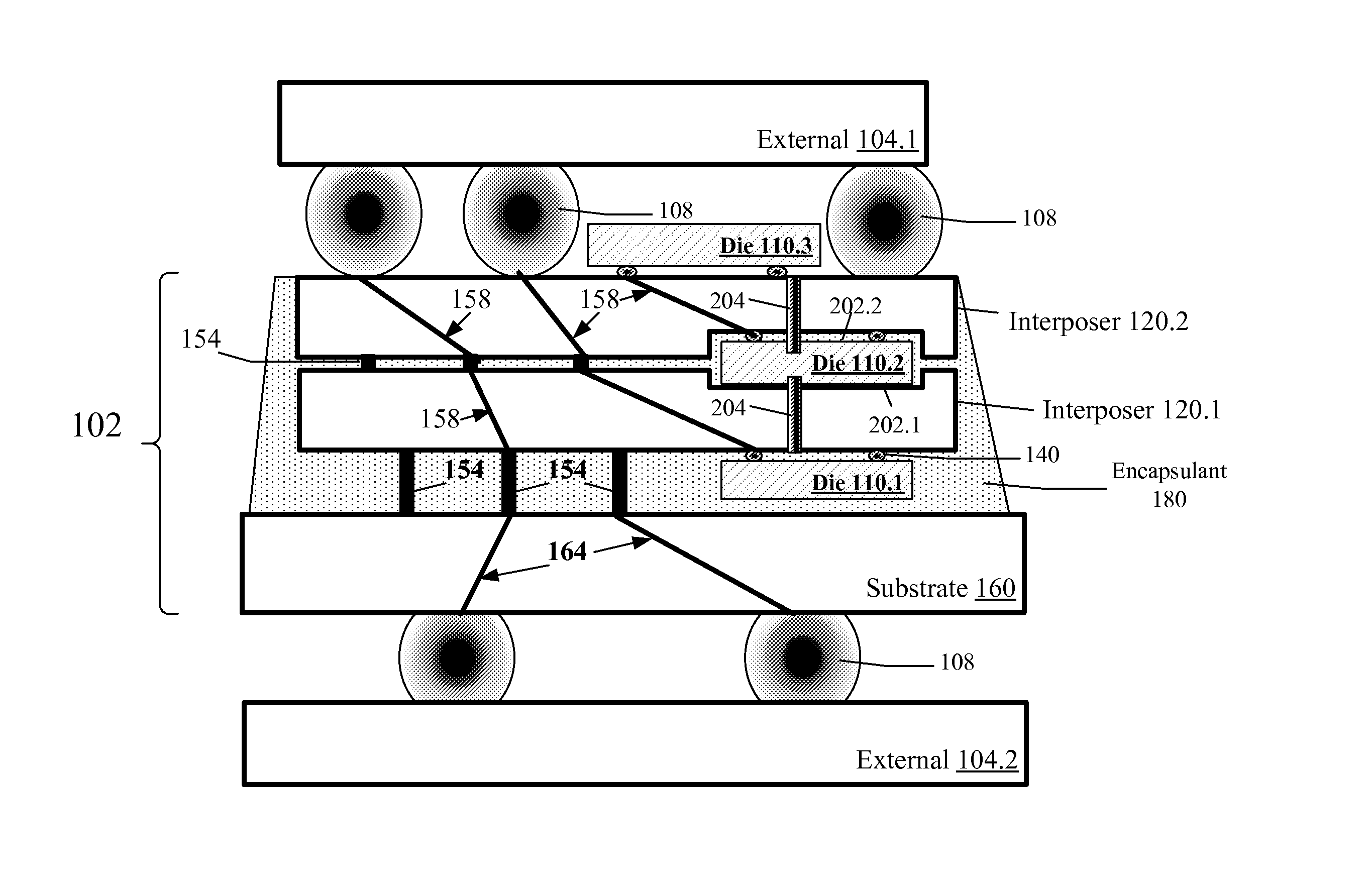
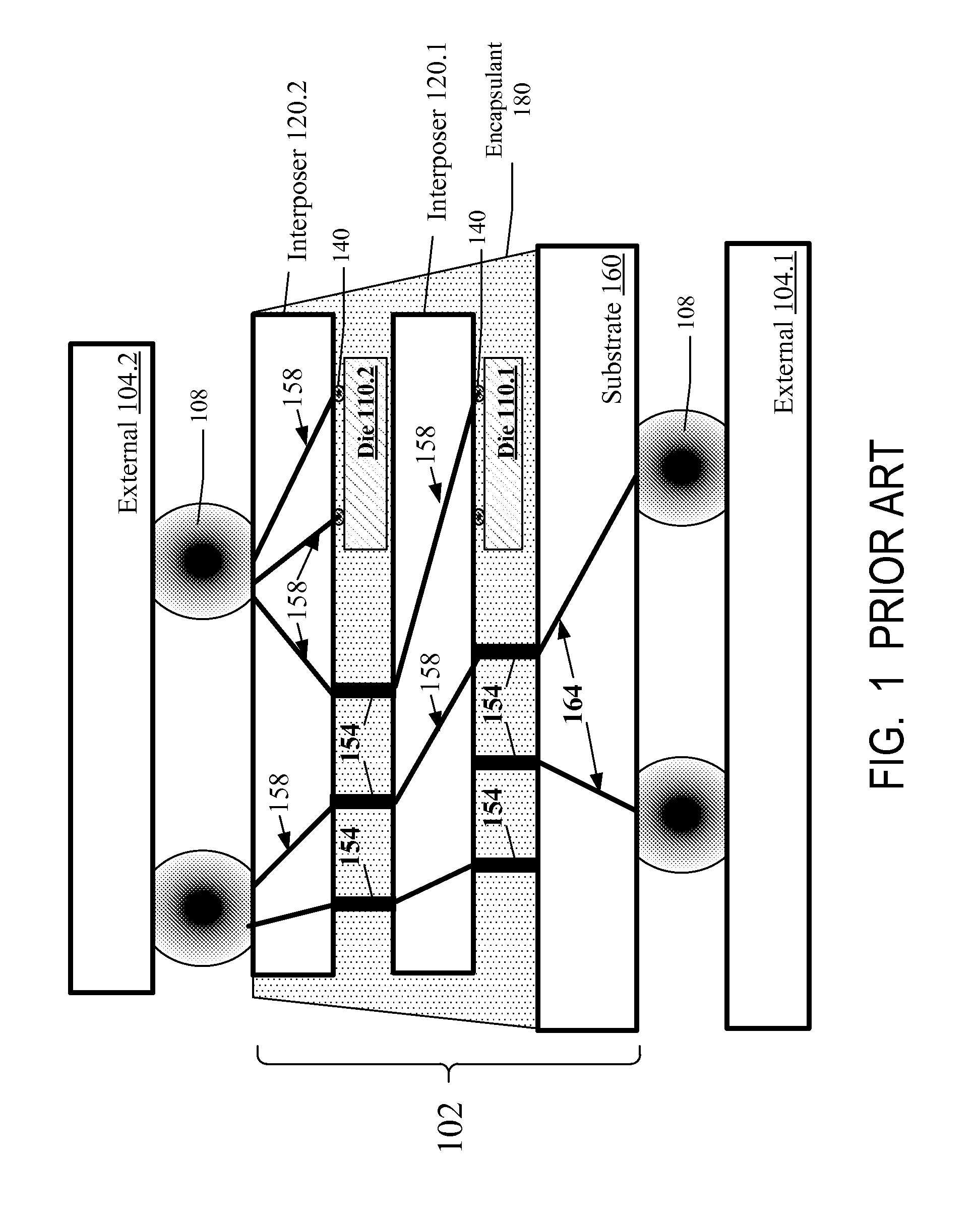
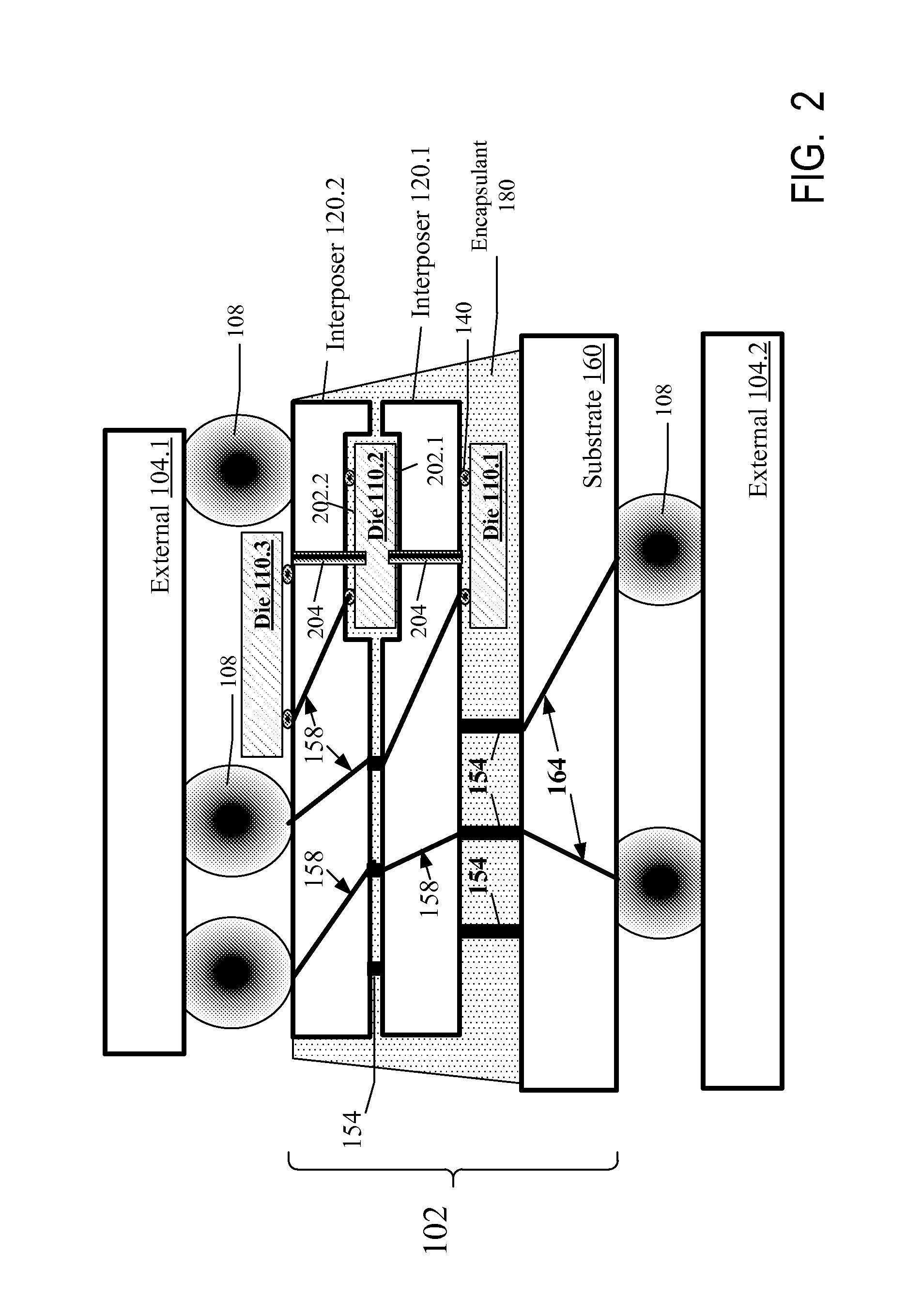
[0018]FIG. 3A shows the beginning stages of fabrication of an interposer 120.1 according to some embodiments of the present invention. The beginning and other stages are similar to those described in U.S. patent application Ser. No. 14 / 214,365, filed Mar. 14, 2014 by Invensas Corporation, and U.S. provisional patent application No. 61 / 952,066, filed Mar. 12, 2014 by Shen et al., both incorporated herein by reference. The interposer substrate 120.1S is initially chosen to be sufficiently thick to provide easy handling and adequate heat dissipation in fabrication. In some embodiments, substrate 120.1S is a monocrystalline silicon wafer of a 200 mm or 300 mm diameter and a thickness of 650 micron or more. These materials and dimensions are exemplary and do not limit the invention. For example, substrate 120.1S can be made of other semiconductor mate...


PUM


Abstract

Semiconductor integrated circuits (110) or assemblies are disposed at least partially in cavities between two interposers (120). Conductive vias (204M) pass through at least one of the interposers or at least through the interposer's substrate, and reach a semiconductor integrated circuit or an assembly. Other conductive vias (204M.1) pass at least partially through multiple interposers and are connected to conductive vias that reach, or are capacitively coupled to, a semiconductor IC or an assembly. Other features are also provided.

Description

BACKGROUND OF THE INVENTION[0001]This document relates to semiconductor integrated circuits (ICs), and more particularly to assemblies with semiconductor integrated circuits.[0002]Multiple ICs can be combined in a high-density assembly to provide needed functionality. High density is desired for small assembly size and also to shorten electrical paths as needed for high speed and low power consumption. However, a small IC is a fragile device with tiny, densely packed contact pads which must be connected to possibly larger contact pads of other integrated or non-integrated (discrete) circuits. To enable such connections, an intermediate IC (interposer) can be provided. Interposers may also increase the mechanical strength of the assembly, absorb stresses generated due to differences in coefficients of thermal expansion (CTE), and improve the ability to dissipate heat that can be generated during operation or manufacture. However, interposers increase the assembly size and complexity,...

Claims


Application Information

Patent Timeline
IPC IPC(8): H01L25/065H01L21/52H01L23/00
CPCH01L25/0652H01L24/83H01L2225/06541H01L21/52H01L2225/06548H01L24/33H01L2224/12105H01L2224/16227H01L2224/73253H01L2224/73259H01L2924/15153H01L2924/15311H01L2924/16235H01L2924/16251H01L2224/92224H01L2225/06527H01L24/73H01L24/92H01L24/94H01L24/97H01L25/50H01L2224/16145H01L2224/17181H01L2224/32145H01L2224/48091H01L2224/48145H01L2224/48227H01L2224/73204H01L2224/73209H01L2224/8182H01L2224/85205H01L2224/9202H01L2224/92125H01L2224/94H01L2224/97H01L2225/06517H01L2225/06589H01L2225/06513H01L2225/06544H01L2225/06524H01L2225/06572H01L23/3121H01L21/561H01L2924/181H01L2224/16225H01L2924/15192H01L2225/1023H01L2225/1058H01L2924/351H01L2224/85H01L2224/81H01L2224/83H01L2924/00H01L2924/00012H01L2924/00014H01L23/49811H01L23/49827H01L23/49844H01L23/5384H01L24/09H01L2224/08165H01L2224/08235
Inventor SHEN, HONGWOYCHIK, CHARLES G.SITARAM, ARKALGUD R.
Owner INVENSAS CORP
Why Eureka
Try Eureka