Semiconductor device and manufacturing method for the same

a technology of semiconductor devices and semiconductors, applied in the direction of semiconductor devices, basic electric elements, electrical equipment, etc., can solve the problem of increasing the active current of soi transistors, and achieve the effect of suppressing the antenna

Inactive Publication Date: 2016-01-14
RENESAS ELECTRONICS CORP
View PDF3 Cites 11 Cited by
  • Summary
  • Abstract
  • Description
  • Claims
  • Application Information

AI Technical Summary

Benefits of technology

[0006]In a semiconductor device including an SOI substrate that performs substrate bias control, a gate electrode of a field-effect transistor (hereinafter “SOI transistor”) formed in a circuit cell portion is electrically connected to a gate electrode of a dummy fill-cell (hereinafter “anti-antenna-effect dummy fill-cell”) formed in a dummy fill-cell portion disposed in a space between circuit c

Problems solved by technology

The structure, however, poses a problem that a gate leak current is generated at the anti-ante

Method used


Image

  • Semiconductor device and manufacturing method for the same
  • Semiconductor device and manufacturing method for the same
  • Semiconductor device and manufacturing method for the same

Examples


first embodiment

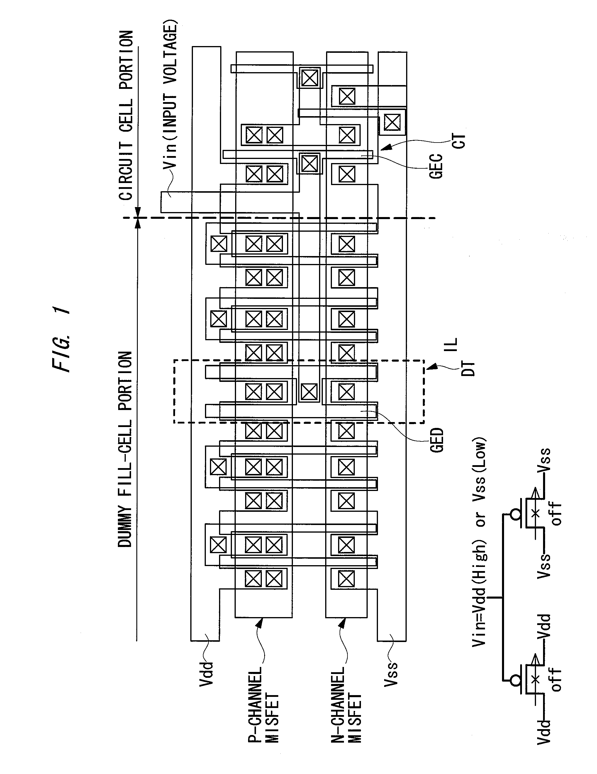
[0041]A semiconductor device including an SOI substrate has a problem that for example, a gate insulating film of an SOI transistor formed in a circuit cell portion is damaged by charged particles accumulated on an interconnect due to plasma-induced damage in a wiring process and this damage to the gate insulating film results in a change in a threshold voltage, etc. This phenomenon is referred to as antenna effect. To improve the reliability of the semiconductor device, suppressing the antenna effect is essential.

[0042]The antenna effect is suppressed in such a way that the charged particles accumulated on the interconnect are dispersed by electrically connecting a gate electrode of the SOI transistor formed in the circuit cell portion to a gate electrode of an anti-antenna-effect dummy fill-cell formed in a dummy fill-cell portion via an interconnect. This method, however, brings another problem that a gate leak current is generated at the anti-antenna-effect dummy fill-cell, lead...

second embodiment

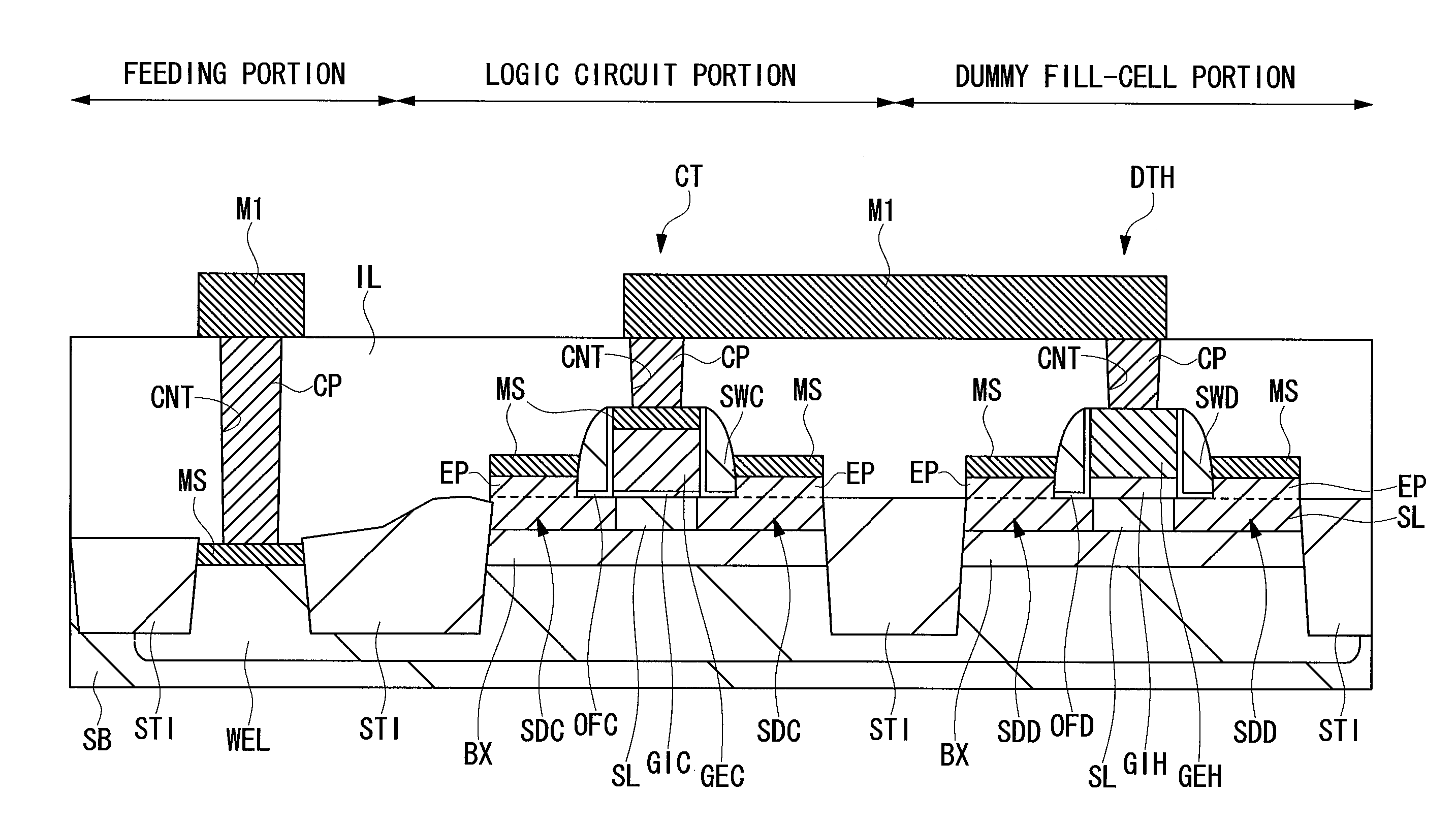
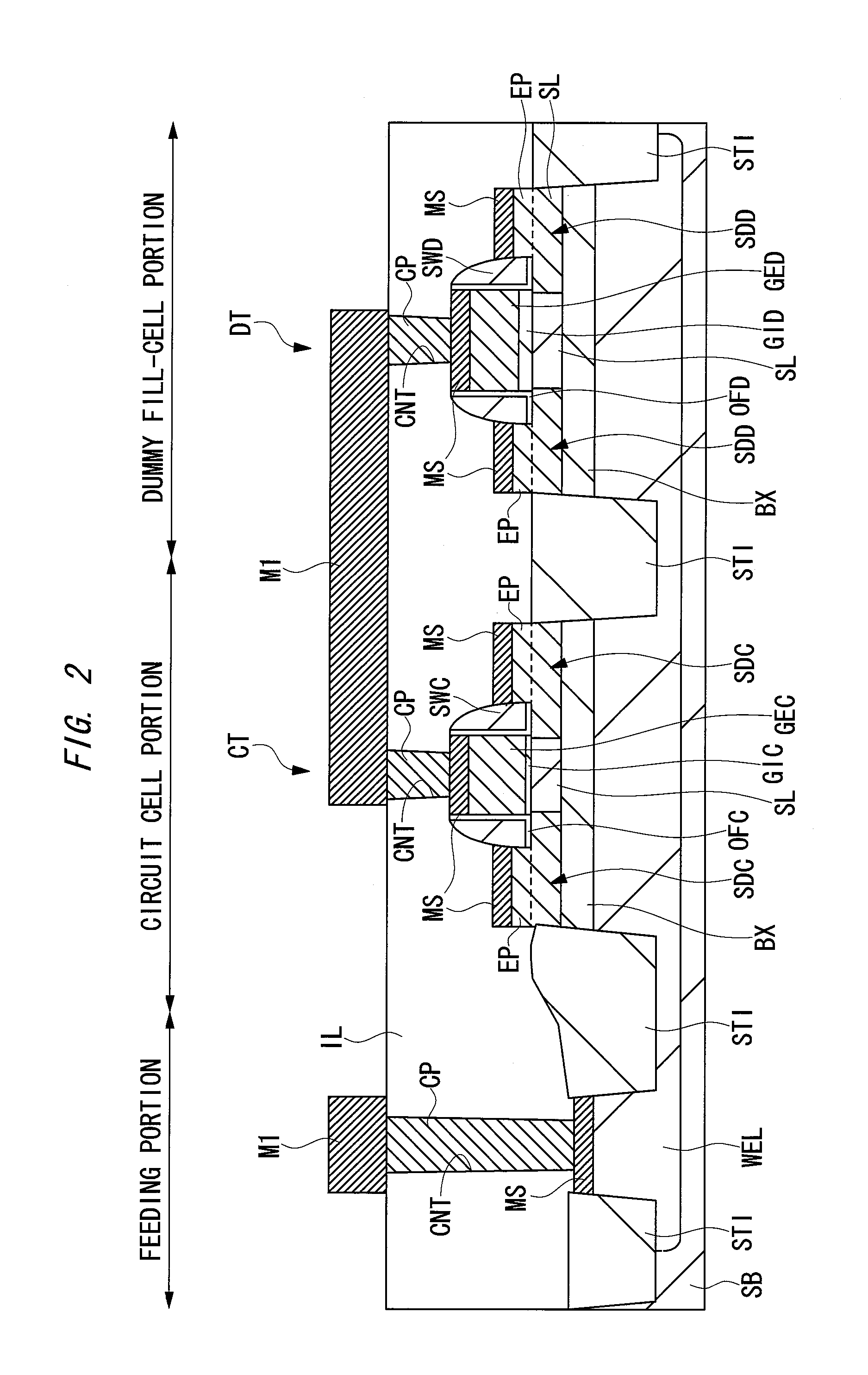
[0125]According to the first embodiment described above, the gate insulating film GID of the anti-antenna-effect dummy fill-cell DT is formed of a silicon oxide film or a silicon oxynitride film, as shown, for example, in FIG. 2. In another embodiment, however, a high dielectric constant film with a dielectric constant higher than that of the silicon nitride film, such as a film made of oxide (metal compound) of any one of Hf (hafnium), Zr (zirconium), Al (aluminum), Ti (titanium), etc., or silicate compound of any one of these substances, may be used in place of the silicon oxide film or the silicon oxynitride film, as the gate insulating film GID.

[0126]FIG. 26 is a cross-sectional view of main parts of a semiconductor device according to a second embodiment.

[0127]As shown in FIG. 26, a gate insulating film GIH of an anti-antenna-effect dummy fill-cell DTH is formed of a high dielectric constant film, while a gate insulating film GIC of the SOI transistor and a gate insulating film...


PUM


Abstract

A semiconductor device including an SOI substrate reduces a gate leak current of an anti-antenna-effect dummy fill-cell and suppresses an antenna effect. The thickness of a gate insulating film of the anti-antenna-effect dummy fill-cell is determined to be large than that of a gate insulating film of an SOI transistor. This reduces the gate leak current of the anti-antenna-effect dummy fill-cell. The gate area (gate length×gate width) of the anti-antenna-effect dummy fill-cell is determined to be large than that (gate length×gate width) of the SOI transistor. This makes the gate capacity of the anti-antenna-effect dummy fill-cell almost equal to that of SOI transistor, thereby suppressing the antenna effect.

Description

CROSS-REFERENCE TO RELATED APPLICATION[0001]The present application claims priority from Japanese Patent Application No. 2014-140183 filed on Jul. 8, 2014, the content of which is hereby incorporated by reference into this application.TECHNICAL FIELD OF THE INVENTION[0002]The present invention relates to a semiconductor device and a manufacturing technique for the same that can be used preferably as, for example, a semiconductor device including an SOI (Silicon on Insulator) substrate and a manufacturing method for the same.BACKGROUND OF THE INVENTION[0003]Japanese Laid-Open Patent Publication No. 2003-133559 (Patent Document 1) describes a technique according to which a first interconnect layer has at least one interconnect connected directly to an impurity diffusion region or connected to the same via an interconnect of an interconnect layer disposed below the first interconnect layer and a first ratio between the area of at least one interconnect and the area of the impurity diff...

Claims


Application Information

Patent Timeline
IPC IPC(8): H01L27/12H01L21/84H01L29/423
CPCH01L27/1203H01L29/42376H01L29/42364H01L21/84H01L29/42368H01L29/78H01L29/78648H01L27/1207H01L29/665
Inventor MAKIYAMA, HIDEKI
Owner RENESAS ELECTRONICS CORP
Why Eureka
Try Eureka