Organic electroluminescent display device, method for manufacturing the same and display apparatus

a technology of electroluminescent display device and organic electroluminescent light, which is applied in the field of display technique, can solve the problems of many manufacturing steps, high cost, time-consuming, complicated production process of conventional oled light device, etc., and achieve the effects of saving production costs, improving production efficiency, and simplifying process steps

Active Publication Date: 2016-01-14
BOE TECH GRP CO LTD
View PDF3 Cites 15 Cited by
  • Summary
  • Abstract
  • Description
  • Claims
  • Application Information

AI Technical Summary

Benefits of technology

[0008]In order to overcome or alleviate at least one aspect of the above mentioned disadvantages, embodiments of the present invention provides an organic electroluminescent display device, a method for manufacturing the same and a display apparatus, which can simplify production process, reduce production cost and shorten production time of the OLED device.
[0010]In the organic electroluminescent display device as described above according to an embodiment of the present invention, since the active layer is made of the transparent oxide semiconductor material and performing the plasma treatment on the oxide semiconductor material may increase concentration of carriers therein, it is possible to use the oxide semiconductor material of which the active layer is made to produce the anode, so that the anode and the active layer are disposed in the same layer. In this way, when producing the OLED device, the active layer and the anode may be simultaneously produced only by changing the pattern of the corresponding mask without additional patterning processes for producing the anodes, thereby simplifying process steps, saving production costs, improving production efficiency and shortening production time.
[0016]In order to save production costs and improve the production efficiency, the organic electroluminescent display device further comprises a metal reflective layer which is disposed in a region corresponding to the organic electroluminescent structure, the metal reflective layer and the gate electrode being disposed in a same layer and made of a same material.
[0019]In the method for producing the organic electroluminescent display device according to the embodiment of the present invention, since the active layer of the thin film transistor and the anode of the organic electroluminescent structure are formed by the single patterning process, the active layer and the anode may be simultaneously produced only by changing the pattern of the corresponding mask without additional patterning process for producing the anode, thereby simplifying process steps, saving production costs, improving production efficiency and shortening production time.
[0020]In the method as described above, the step of forming the thin film transistor on the substrate comprises: forming the gate electrode on the substrate; forming the active layer on the substrate formed with the gate electrode; and forming the source electrode and the drain electrode on the substrate formed with the active layer, wherein a metal reflective layer is formed in a region on the substrate corresponding to the organic electroluminescent structure while forming the gate electrode on the substrate. In this way, it is possible to further simplify production process, saving production costs and improve production efficiency.

Problems solved by technology

Therefore, the manufacturing process of the conventional OLED devices has problems of complicated production process, many manufacturing steps, high cost, time-consuming and the like.

Method used


Image

  • Organic electroluminescent display device, method for manufacturing the same and display apparatus
  • Organic electroluminescent display device, method for manufacturing the same and display apparatus
  • Organic electroluminescent display device, method for manufacturing the same and display apparatus

Examples


Embodiment Construction

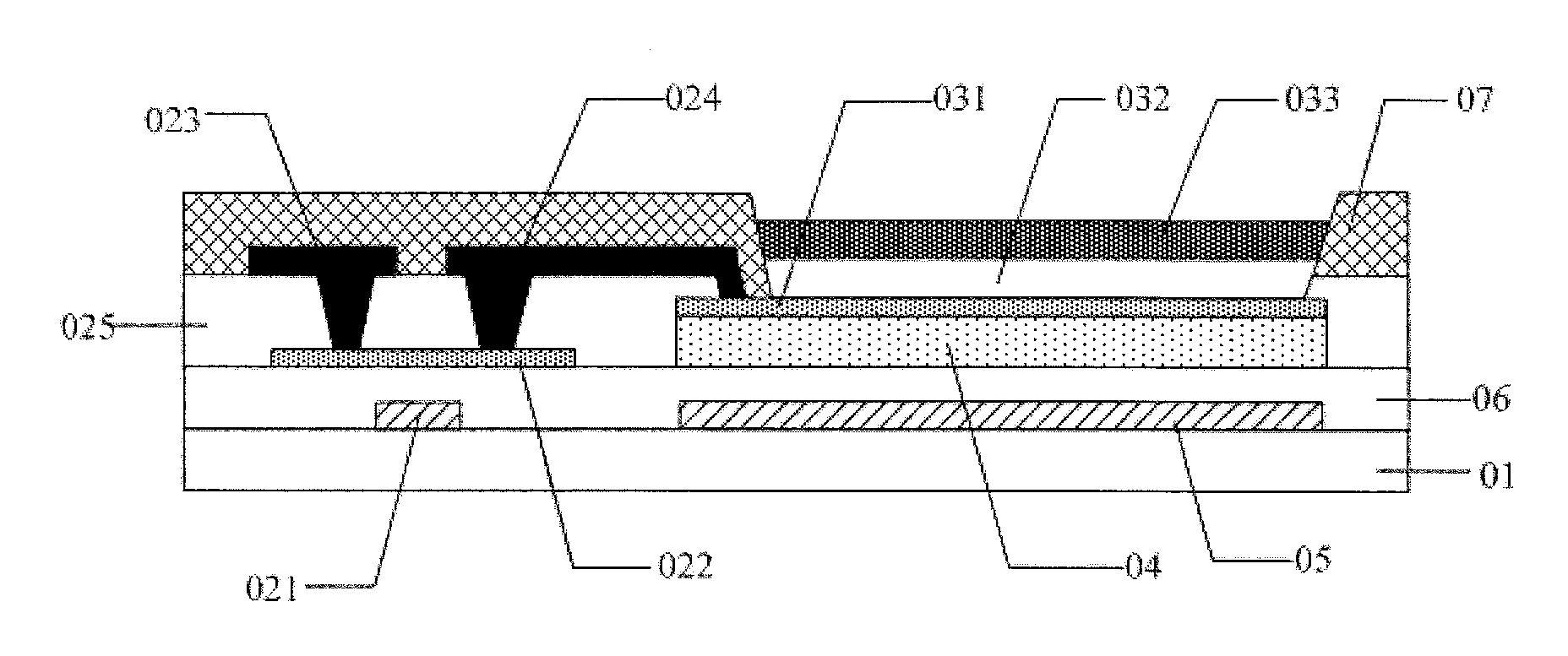
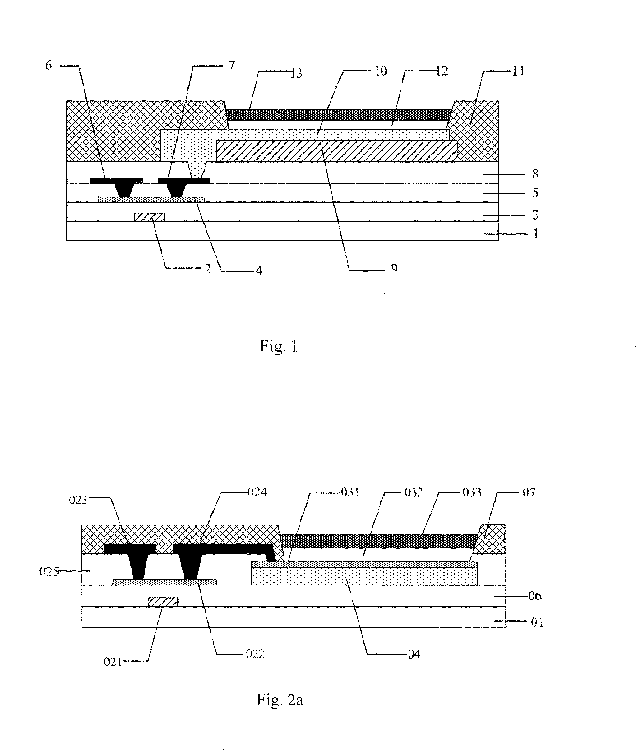
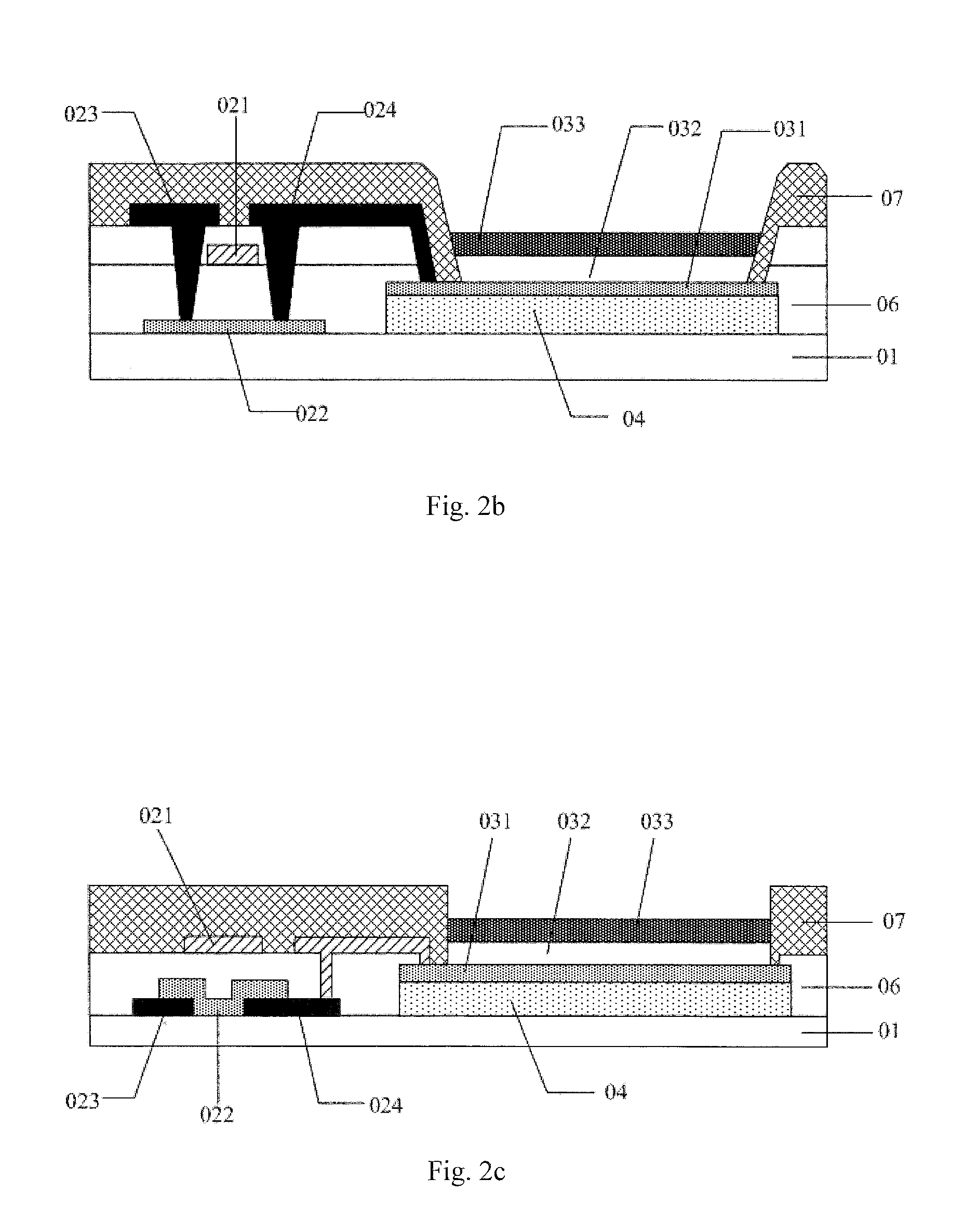
[0028]In order to completely understand the technical solution of the present invention, exemplary embodiments of the present disclosure will be described hereinafter in detail with reference to the attached drawings. Obviously, the described embodiments are merely part of the embodiments of the present invention, rather than all of the embodiments of the present invention. Based on the embodiments of the present invention, other embodiments acquired by the person skilled in the art without any inventive effort will be within the protection scope of the present invention.

[0029]The shape and size of each film layer in the attached drawings do not represent the real scale of the OLED device. Moreover, only partial structures of the OLED device are shown and are intended to schematically illustrate the content of the present invention. In addition, in the following detailed description, for purposes of explanation, numerous specific details are set forth in order to provide a thorough ...


PUM


Abstract

Disclosed is an organic electroluminescent display device, a method for manufacturing the same and a display apparatus. The organic electroluminescent display device comprises: a substrate; a thin film transistor disposed on the substrate and including a gate electrode and an active layer insulated with each other, and a source electrode and a drain electrode connected with the active layer; and an organic electroluminescent structure disposed on the substrate and including an anode, a luminescent layer and a cathode stacked sequentially, the anode and the drain electrode being electrically connected with each other. The anode and the active layer are disposed in the same layer. The active layer is made of a transparent oxide semiconductor material. The anode is made of the transparent oxide semiconductor material undergone a plasma treatment. When producing the OLED device, the active layer and the anode may be simultaneously produced only by changing the pattern of the corresponding mask without additional patterning processes for producing the anodes, thereby simplifying process steps and saving production costs.

Description

BACKGROUND OF THE INVENTION[0001]1. Field of the Invention[0002]Embodiments of the present invention generally relate to field of display technique, particularly to an organic electroluminescent display device, a method for producing the same and a display apparatus.[0003]2. Description of the Related Art[0004]Currently, an organic electroluminescent display (OLED) device has been widely used in a display apparatus due to its characteristics of quick response, wide color gamut, ultrathin structure, and the capability of becoming flexible and the like as compared to a conventional liquid crystal display (LCD) device.[0005]The OLED device generally comprises a thin film transistor array substrate and an organic electroluminescent structure. In the OLED device, a thin film transistor generally includes a gate electrode, an active layer, a source electrode and a drain electrode. The organic electroluminescent structure generally includes an anode, a luminescent layer and a cathode. Spec...

Claims


Application Information

Patent Timeline
Patent Type & Authority Applications(United States)
IPC IPC(8): H01L27/32H01L51/00H01L29/24H01L29/417H01L29/423H01L29/66H01L29/786H01L51/52H01L51/56
CPCH01L51/0023H01L27/3248H01L29/7869H01L51/5206H01L27/322H01L51/5271H01L2227/323H01L51/56H01L29/66969H01L29/42384H01L29/41733H01L29/24H01L27/3262H01L27/3276H01L27/1225H01L27/127H10K59/38H10K59/123H10K59/1213H10K50/856H10K71/621H10K50/81H10K59/131H10K71/00H10K59/1201
Inventor REN, ZHANGCHUN
Owner BOE TECH GRP CO LTD
Why Eureka
Try Eureka