Organic photoelectronic device and image sensor

an image sensor and photoelectronic technology, applied in the direction of solid-state devices, semiconductor devices, thermoelectric devices, etc., can solve the problems of deterioration of sensitivity and widespread use of silicon photodiodes, and achieve the effect of improving wavelength selectivity and improving spectral characteristics

Active Publication Date: 2016-01-21
SAMSUNG ELECTRONICS CO LTD
View PDF3 Cites 22 Cited by
  • Summary
  • Abstract
  • Description
  • Claims
  • Application Information

AI Technical Summary

Benefits of technology

[0008]At least one example embodiment relates to an organic photoelectronic device capable of improving wavelength selectivity due to improved spectral characteristics.

Problems solved by technology

At present, silicon photodiodes are widely used, but typically exhibit deteriorated sensitivity because of a small absorption area due to small pixels.

Method used


Image

  • Organic photoelectronic device and image sensor
  • Organic photoelectronic device and image sensor
  • Organic photoelectronic device and image sensor

Examples


example 1

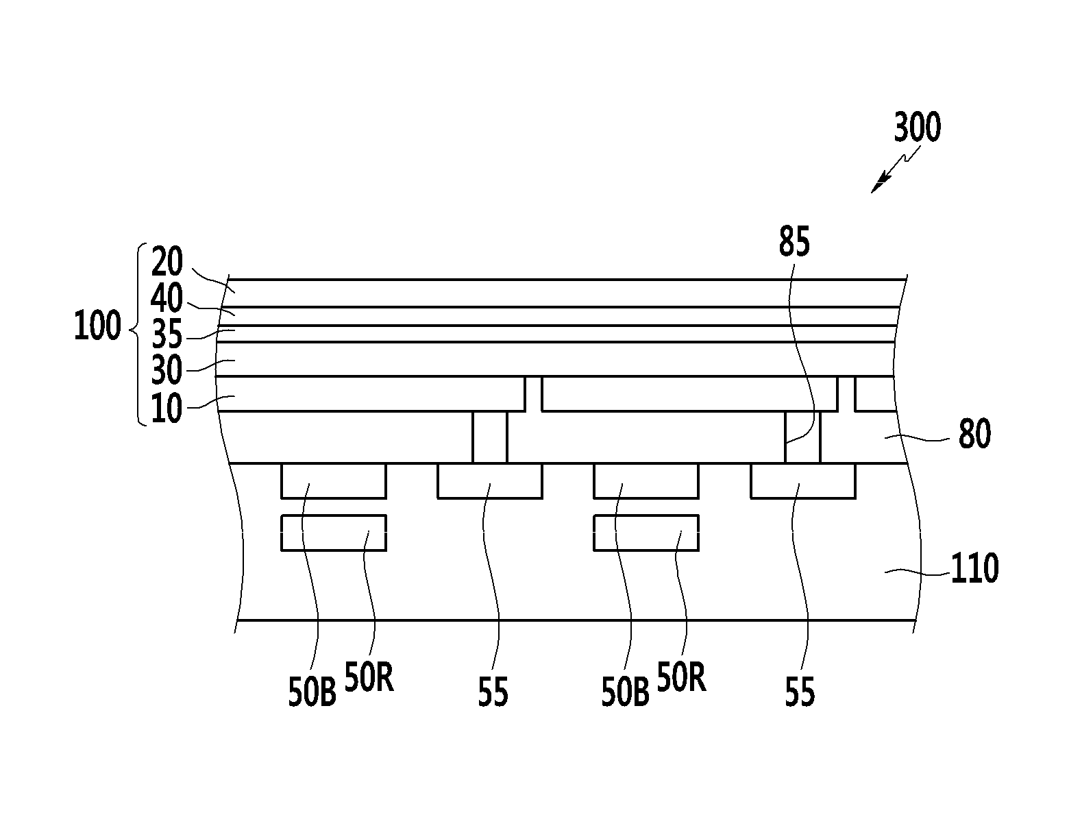
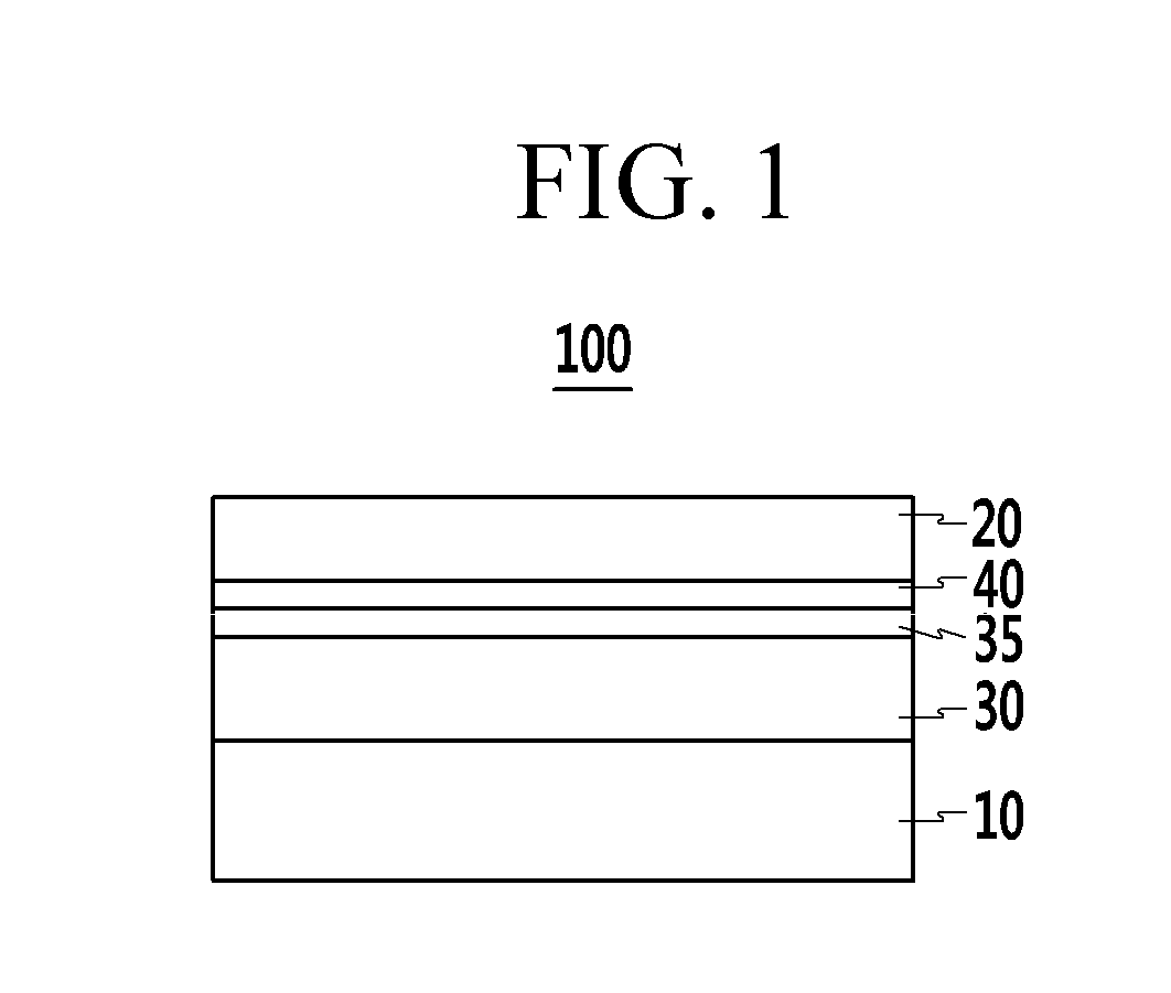
[0131]ITO is sputtered on a glass substrate to form an approximately 100 nm-thick lower electrode. Subsequently, molybdenum oxide (MoOx, 0

example 2

[0132]An organic photoelectronic device is manufactured according to the same method as Example 1, except for using fullerene (C60) instead of the dicyanovinyl-terthiophene (DCV3T) as the n-type light-absorption material.

example 3

[0133]An organic photoelectronic device is manufactured according to the same method as Example 1, except for using fullerene (C60) instead of the dicyanovinyl-terthiophene (DCV3T) as the n-type light-absorption material of the light-absorption layer, and a compound represented by the following Chemical Formula 1b instead of the compound represented by the above Chemical Formula 1a for the light-absorption auxiliary layer.

[0134]The compound represented by the above Chemical Formula 1 b is synthesized by the following method.

[0135]20.0 g of boron sub-phthalocyanine chloride, 32.0 g of triphenylsilanol, and 14.8 g of trifluoromethanesulfonic acid are heated and refluxed in 150 ml of dry toluene for 15 hours. Then, 200 ml of methylene chloride is added to the resultant, the mixture is filtered, and the filtered solution is concentrated under a reduced pressure and purified through silica gel column chromatography, obtaining a compound represented by the above Chemical Formula 1 b.


PUM


Abstract

Example embodiments relate to an organic photoelectronic device that includes a first electrode, a light-absorption layer on the first electrode and including a first p-type light-absorption material and a first n-type light-absorption material, a light-absorption auxiliary layer on the light-absorption layer and including a second p-type light-absorption material or a second n-type light-absorption material that have a smaller full width at half maximum (FWHM) than the FWHM of the light absorption layer, a charge auxiliary layer on the light-absorption auxiliary layer, and a second electrode on the charge auxiliary layer, and an image sensor including the same.

Description

[0001]This application claims the benefit of priority to Korean Patent Application No. 10-2014-0089914 filed in the Korean Intellectual Property Office on Jul. 16, 2014, the entire contents of which are incorporated herein by reference.BACKGROUND[0002]1. Field[0003]Example embodiments relate to an organic photoelectronic device and an image sensor.[0004]2. Description of the Related Art[0005]A photoelectronic device typically converts light into an electrical signal using photoelectronic effects, may include a photodiode, a phototransistor, and the like, and may be applied to an image sensor, a solar cell, and the like.[0006]An image sensor including a photodiode requires high resolution and thus a small pixel. At present, silicon photodiodes are widely used, but typically exhibit deteriorated sensitivity because of a small absorption area due to small pixels. Accordingly, an organic material that is capable of replacing silicon has been researched.[0007]Accordingly, an organic mate...

Claims


Application Information

Patent Timeline
Patent Type & Authority Applications(United States)
IPC IPC(8): H01L27/30H01L51/00
CPCH01L27/307H01L51/44H01L51/0094H01L51/008Y02E10/549H10K39/00H10K30/57H10K30/211H10K30/20H10K30/30H01L25/167H01L33/06H10K39/32H10K30/82H10K30/87H10K85/40H10K85/322H10K30/80H10K85/211H10K85/655
Inventor PARK, KYUNG BAERYUICHI, SATOHLEE, GAE HWANGLEE, KWANG HEELEEM, DONG-SEOKJIN, YONG WANYAGI, TADAOHEO, CHUL JOON
Owner SAMSUNG ELECTRONICS CO LTD
Why Eureka
Try Eureka