
Tandem Kesterite-Perovskite Photovoltaic Device

a photovoltaic device and kesterite technology, applied in the field of kesterite-perovskite photovoltaic devices, can solve the problems of less strict processing and current matching requirements of four-terminal tandem devices, less frequent use of configuration in practice, and more difficult fabrication of two-terminal tandem devices

Inactive Publication Date: 2016-02-04
IBM CORP
View PDF8 Cites 28 Cited by
  • Summary
  • Abstract
  • Description
  • Claims
  • Application Information

AI Technical Summary

Benefits of technology

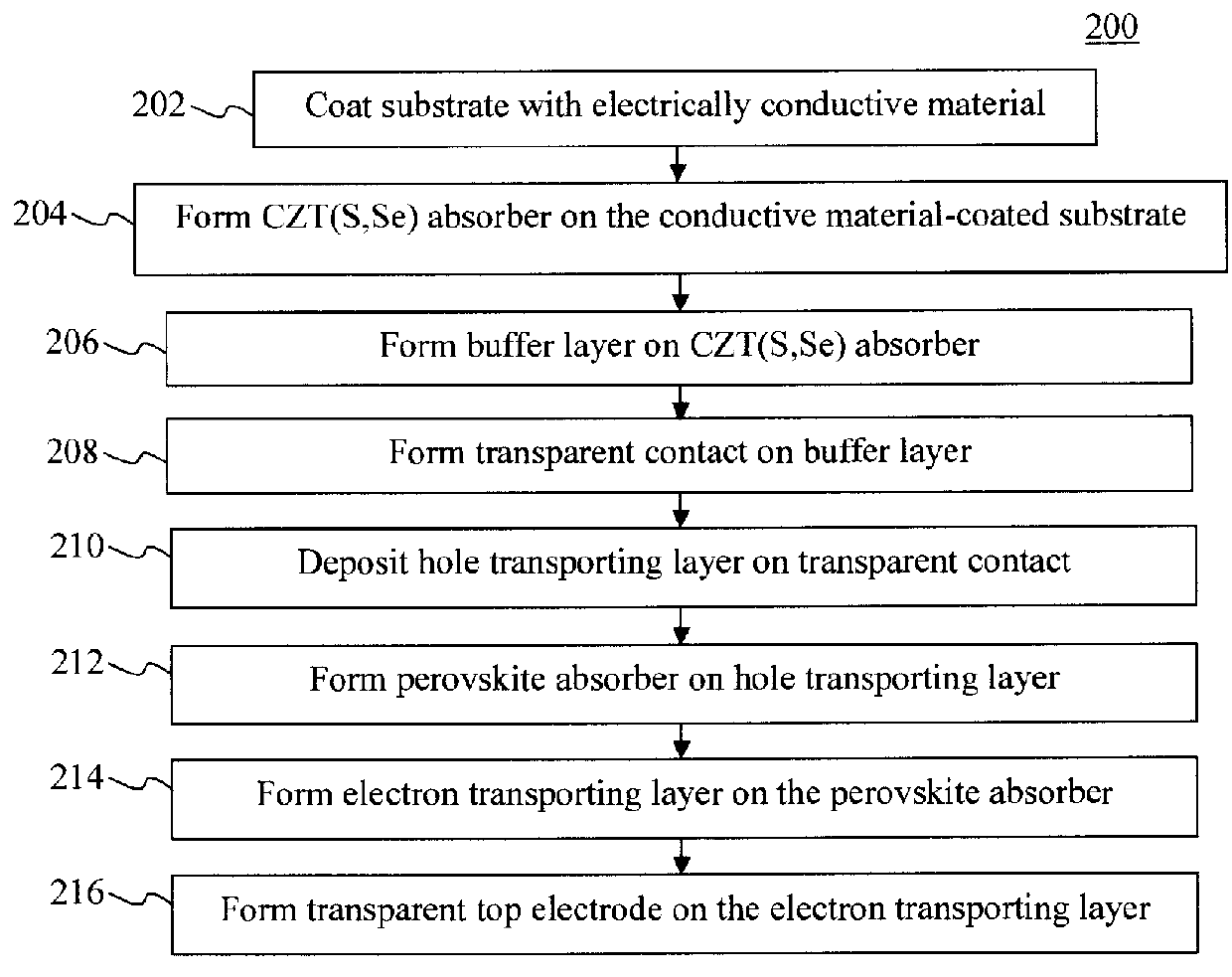
The present invention provides tandem Kesterite-perovskite photovoltaic devices and techniques for their formation. The devices consist of a bottom cell with a first absorber layer and a top cell with a second absorber layer. The first absorber layer includes copper, zinc, tin, and at least one of sulfur and selenium, while the second absorber layer includes a perovskite material. The devices have improved efficiency and can generate electricity from sunlight. The methods for their formation involve coating a substrate with a layer of electrically conductive material, sequentially adding layers of absorber, buffer, hole transporting, electron transporting, and a transparent top electrode on the substrate. This invention allows for the production of more efficient photovoltaic devices.

Problems solved by technology

Three-terminal tandem devices have also been demonstrated (i.e., those having a top cell and a bottom cell which share an electrode in the middle) but this configuration is not often used in practice.
Two-terminal tandem devices are more challenging to fabricate than four-terminal devices due to current-matching requirements as well as the need to preserve the performance of the bottom cell during processing of the top cell.
Four-terminal tandem devices have less strict processing and current matching requirements than two-terminal devices, but suffer from significant resistance and optical losses due to the need for multiple transparent conductive contacts and reflection losses associated with adding additional substrates and layers.
Therefore, chalcogenide solar cells cannot be employed as a top cell in a tandem structure due to their low band gaps and the fact that most conventional solar cell devices would deteriorate at the processing temperatures required for forming high-performance absorber materials.
However, these devices typically suffer from low open-circuit voltage (Voc) values.

Method used


Image

  • Tandem Kesterite-Perovskite Photovoltaic Device
  • Tandem Kesterite-Perovskite Photovoltaic Device
  • Tandem Kesterite-Perovskite Photovoltaic Device

Examples


Embodiment Construction

[0020]A tandem, i.e., multi-junction, photovoltaic device architecture allows the combined two-cell stack to achieve high open-circuit voltages (Voc) reaching a maximum value of the sum of the two individual cell voltages. The total short-circuit current density produced by the tandem device is limited by whichever of the individual cells produces the lower current density.

[0021]Provided herein is a two-terminal, two-cell tandem photovoltaic device having a copper zinc tin sulfo-selenide (CZT(S,Se))-based bottom cell and a perovskite-based top cell. It is shown in accordance with the present techniques that the open-circuit voltage of the present tandem device is indeed larger than either of the individual cells and approaches the sum of the two individual Voc values, thereby demonstrating the tandem concept.

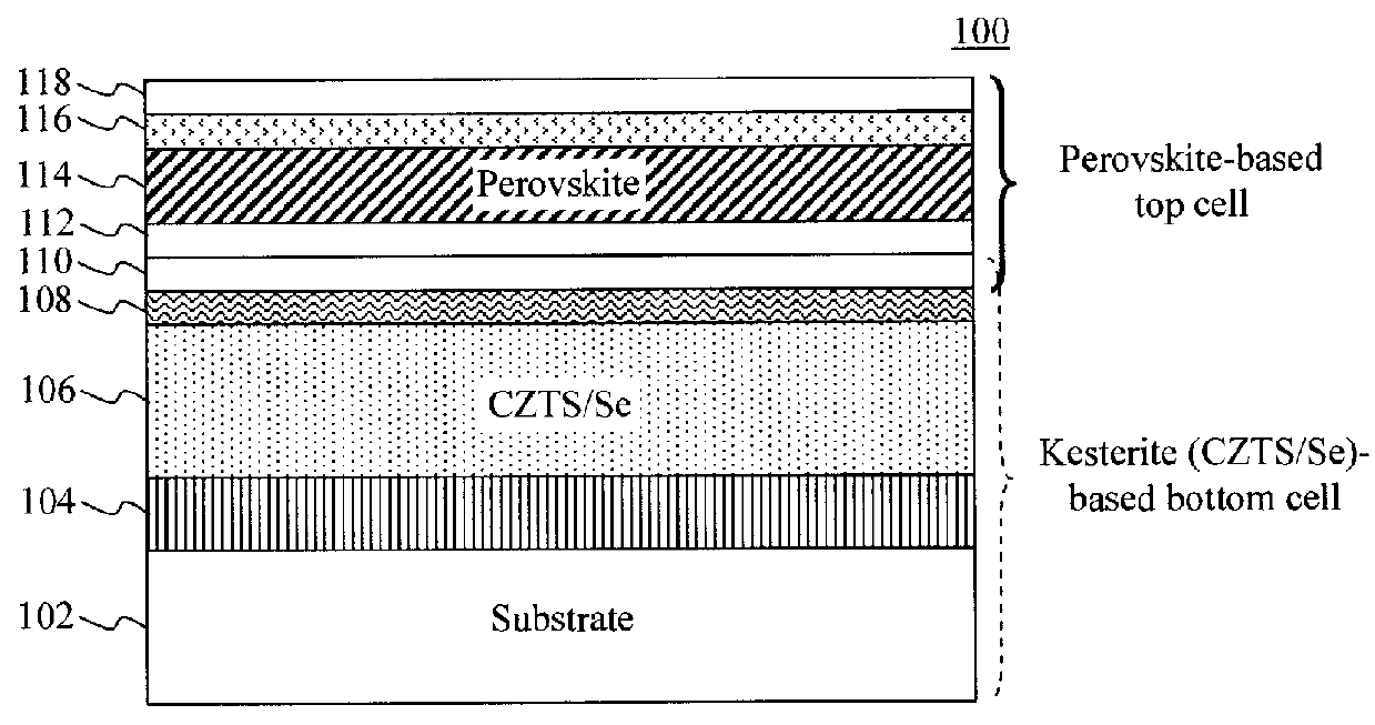
[0022]FIG. 1 is a diagram illustrating an exemplary two-terminal, two-cell tandem photovoltaic device 100 according to the present techniques. As shown in FIG. 1, the device 100...


PUM

PropertyMeasurementUnit
temperatureaaaaaaaaaa
temperaturesaaaaaaaaaa
band gapsaaaaaaaaaa

Abstract

Tandem Kesterite-perovskite photovoltaic devices and techniques for formation thereof are provided. In one aspect, a tandem photovoltaic device is provided. The tandem photovoltaic device includes a bottom cell having a first absorber layer comprising copper, zinc, tin, and at least one of sulfur and selenium and a top cell connected in series with the bottom cell, the top cell having a second absorber layer comprising a perovskite material. A method of forming a tandem photovoltaic device is also provided.

Description

FIELD OF THE INVENTION[0001]The present invention relates to tandem photovoltaic devices and more particularly, to tandem Kesterite (e.g., CZT(S,Se))-perovskite photovoltaic devices and techniques for formation thereof.BACKGROUND OF THE INVENTION[0002]Tandem photovoltaic devices, i.e., multi-junction solar cells based on at least two absorbers with different band gaps, allow broader-spectrum light harvesting and superior photovoltaic conversion efficiency in comparison to single-junction solar cells. Typical configurations include the layers of the tandem device oriented in a stack. For optimal performance, the band gap of the top solar cell absorber in the stack should be higher than that of the bottom cell.[0003]The two most commonly employed groups of tandem device are: (1) two-terminal devices (i.e., those containing one electrode on top and one electrode on bottom, with a tunnel junction between top and bottom cells) and (2) four-terminal devices (i.e., those containing indepen...

Claims


Application Information

Patent Timeline
Patent Type & Authority Applications(United States)
IPC IPC(8): H01L31/0725H01L31/0224H01L31/0296H01L31/032H01L31/074H01L31/18H01L51/00H01L51/42H01L51/44
CPCH01L31/0725H01L51/4273H01L51/442H01L31/074H01L31/0296H01L31/0326H01L2031/0344H01L31/022475H01L31/18H01L51/4213H01L51/0043H01L51/0067H01L31/022425H01L31/072H01L31/078Y02E10/549H10K30/57H10K85/1135H10K85/215H10K30/10H10K30/82H10K85/50Y02E10/50H10K85/654
Inventor GERSHON, TALIA S.GUHA, SUPRATIKGUNAWAN, OKILI, NINGTODOROV, TEODOR K.
Owner IBM CORP
Learn More