Stress Relieved High Power RF Circuit

a high-power, stress-free technology, applied in the direction of waveguides, paper/cardboard containers, containers, etc., can solve the problems of low maximum power handling ability of softboard based rf circuits, low cost, and energy dissipation, and achieve low thermal stress, good electrical performance, and high thermal conductivity and mot

Active Publication Date: 2016-02-18
TTM TECH INC
View PDF0 Cites 2 Cited by
  • Summary
  • Abstract
  • Description
  • Claims
  • Application Information

AI Technical Summary

Benefits of technology

[0017]The present invention addresses the needs described above by providing an RF device that provides good electrical performance and exhibits low thermal stress, while providing relatively high thermal conductivity and MOT. For example, the coupler of the present invention can handle average RF power in excess of 1,000 Watts (W). The present invention is directed to an RF coupler that provides improved reliability at lower cost by substantially minimizing or eliminating solder joint interfaces (by replacing I/O printed circuit board solde

Problems solved by technology

Finally, softboard devices are amenable to being manufactured in large batches, which typically results in lower costs.
On the other hand, the maximum power handling ability of softboard based RF circuits is relatively low because they are characterized by relatively poor thermal conductivity and poor Maximum Operating Temperature (MOT).
Accordingly, one drawback to this approach is that the thermal energy is dissipated over a rather small surface area, and as a result, the thermal energy builds up over time and becomes problematic.
Stated differently, the amount of power that a device can handle is limited by its heat dissipation capabilities.
While these devices offer some convenience, they exhibit power handling limitations (e.g., up to 100-200 W) that are due to thermal resistance and maximum operating temperature (MOT) limitations.
On the other hand, the maximum power handling of ceramic RF devices is limited by electrical performance (where insertion loss is typically higher than similar PCB devices) and solder joint failure (due to reflow or cracked solder joint) at the device-to-carrier PCB interface (solder joint reflow often leads to failed solder joints).
In the solder reflow failure mode, the RF power flowing through the device can cause an all-ceramic RF device to become so hot that the solder reflows and the device separates from the carrier PCB.
Thus, the high thermal conductivity of conventional ceramic devices can lead to device failure if the power level

Method used


Image

  • Stress Relieved High Power RF Circuit
  • Stress Relieved High Power RF Circuit
  • Stress Relieved High Power RF Circuit

Examples


Embodiment Construction

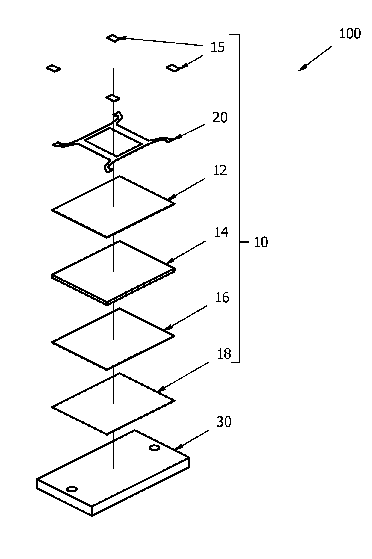
[0064]Reference will now be made in detail to the present exemplary embodiments of the invention, examples of which are illustrated in the accompanying drawings. Wherever possible, the same reference numbers will be used throughout the drawings to refer to the same or like parts. An exemplary embodiment of the stress relieved high power circuit of the present invention is shown in FIG. 5A, and is designated generally throughout by reference numeral 10.

[0065]As embodied herein, and depicted in FIG. 5A, a cross-sectional diagram of an RF coupler 10 in accordance with one embodiment of the present invention is disclosed. Specifically, a circuit layer 20 is disposed overtop a laminate comprised of various layers of dielectrics including low modulus dielectric layer 12, ceramic core 14, and another low modulus dielectric layer 16. A conductive ground plane 18 is disposed on the underside of the dielectric layer 16 to complete the microstrip circuit. In one version of this embodiment, the...


PUM

PropertyMeasurementUnit
Temperature coefficient of resistanceaaaaaaaaaa
Temperatureaaaaaaaaaa

Abstract

The present invention is directed to an RF device that includes a laminate structure having a ceramic layer having a predetermined thermal conductivity that is a function of a predetermined RF device operating temperature. The ceramic layer forms a first major surface of the laminate structure and a second major ceramic surface is bonded to a layer of thermoplastic material that is, in turn, bonded to a conductive layer. The thermoplastic material has a coefficient of thermal expansion that substantially matches the conductive layer. A first circuit arrangement is disposed on the first major surface of the laminate structure and it includes a first RF circuit structure having a predetermined geometry and predetermined electrical characteristics. The laminate structure is configured to dissipate thermal energy generated by the at least one first RF circuit structure via substantially the entire second major surface of the laminate structure.

Description

BACKGROUND OF THE INVENTION[0001]1. Field of the Invention[0002]The present invention relates generally to RF devices, and particularly to relatively high power RF devices with improved thermal characteristics.[0003]2. Technical Background[0004]The primary use of some mobile phones (e.g., smartphones) is data communications rather than voice communications. More and more of the public is using their mobile telephones for Internet access, social media access and for downloading videos and pictures from both of these sources. Thus, the demand for mobile data services is growing at an exponential rate. This necessarily means that the bandwidth provided by the telecommunications infrastructure (as well as the mobile telephone handset itself) must continue to grow if it is to keep pace with the demand. In order to accomplish this, new mobile telephone handsets and new base station equipment must be configured to operate over multiple frequency bands and communications systems (e.g., Wi-F...

Claims


Application Information

Patent Timeline
IPC IPC(8): H01P3/08H01P11/00
CPCH01P11/003H01P3/081H01L23/49833H01L23/66H01P1/20345H05K1/036H01L2223/6627H01P3/088H01P5/227H01L2924/0002H05K3/0061H05K1/0203H05K1/0243H01L2924/00
Inventor OSTERGAARD, HANS P.LEN, MICHAEL J.MEI, CHONGBUYEA, BRIAN K.
Owner TTM TECH INC
Why Eureka
Try Eureka