

Efuse structure with stressed layer
a fuse structure and stressed layer technology, applied in the direction of semiconductor devices, semiconductor/solid-state device details, electrical apparatus, etc., can solve the problem that the fuse structure of fig. 2 does not meet the fast programming requirements of certain applications, and achieve the effect of reducing the required programming time and fast programming speed
- Summary
- Abstract
- Description
- Claims
- Application Information
AI Technical Summary
Benefits of technology
Problems solved by technology
Method used
Image

Examples
embodiment 1
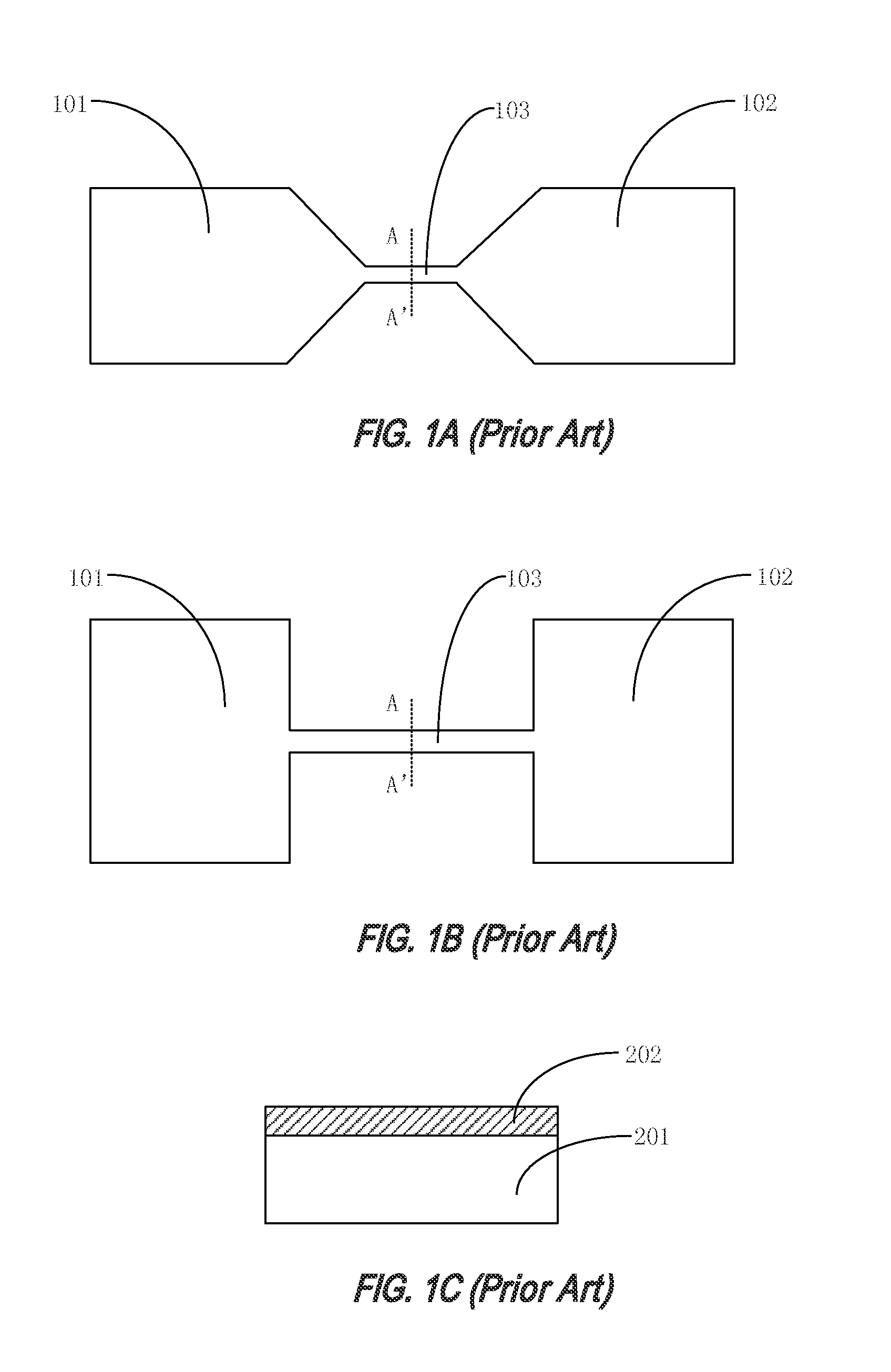
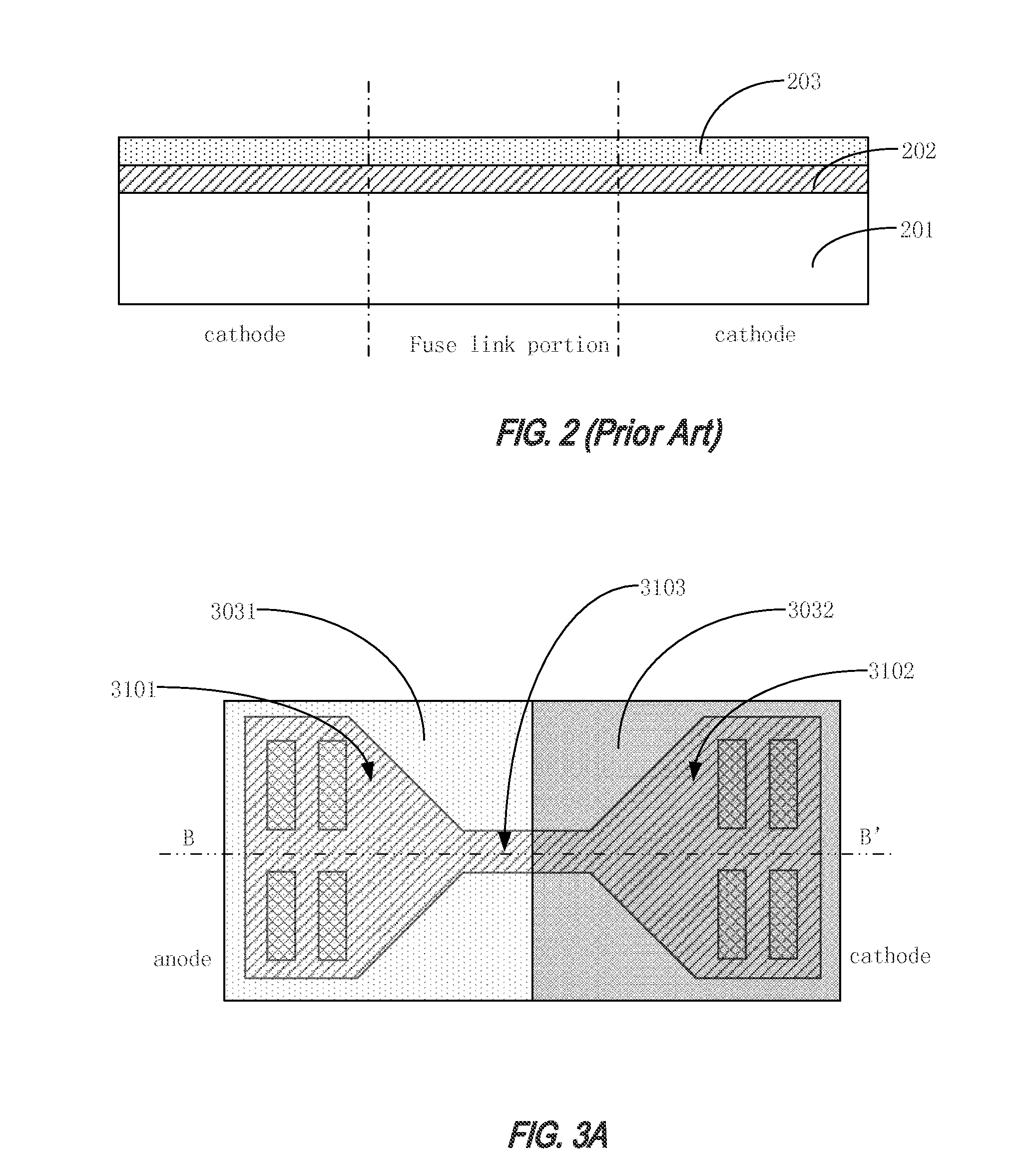
[0038]Referring to FIGS. 3A, 3B and 3C, an electrically programmable fuse (eFuse) device will be described. FIG. 3A is a plan view of an eFuse device according to an embodiment of the present invention. FIG. 3B is a plan view of an eFuse device according to another embodiment of the present invention. FIG. 3C is a cross-sectional view illustrating an exemplary structure of an eFuse device taken along the line BB′ of FIGS. 3A and 3B.
[0039]As shown in FIGS. 3A, 3B and 3C, the eFuse device may include a polycrystalline silicon layer 301 and a silicide layer 302 disposed on polycrystalline silicon layer 301.
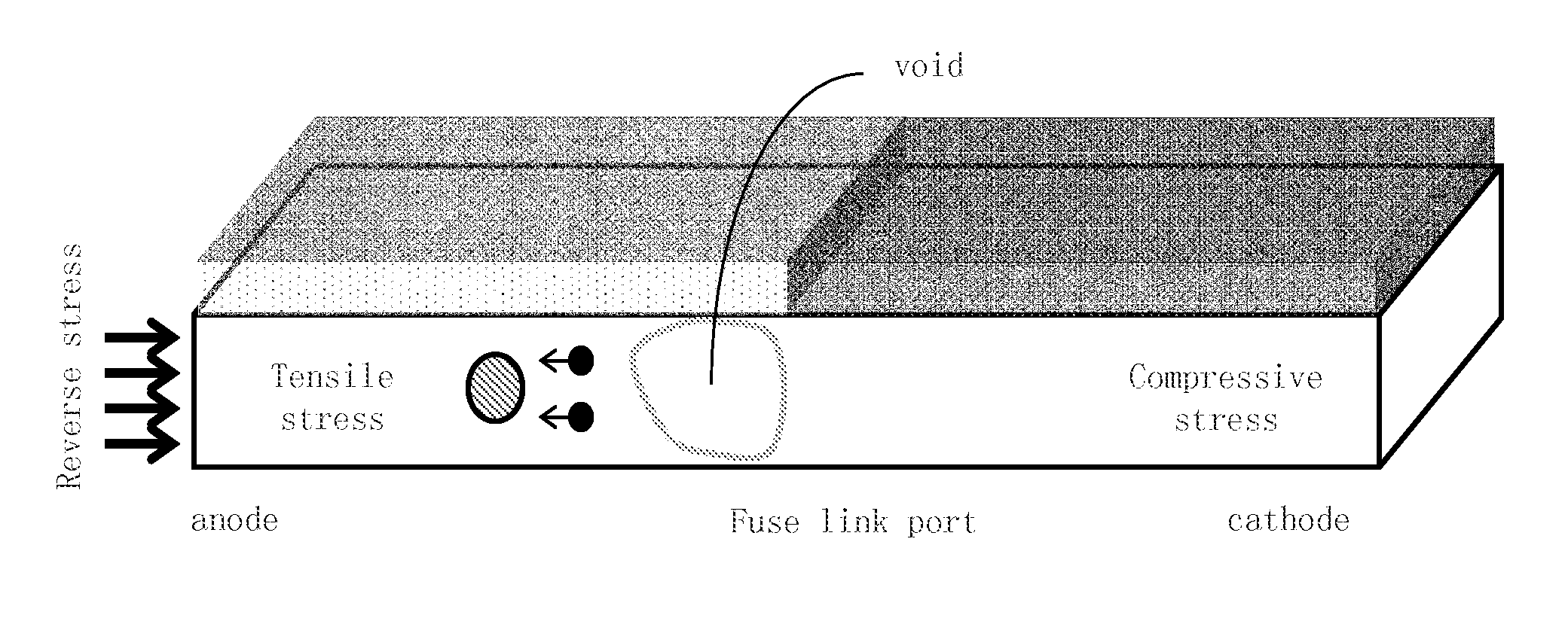
[0040]Polycrystalline silicon layer 301 and silicide layer 302 form an anode 3101, a cathode 3102, and a fuse link portion 3103 connecting anode 3101 and cathode 3102. The eFuse device also includes a compressive stress layer 3031 disposed on anode 3101 and covering anode 3101 and a tensile stress layer 3032 disposed on cathode 3102 and covering cathode 3102.
[0041]Compressive stress ...
embodiment 2
[0056]Embodiments of the present invention provide an integrated circuit that includes an electrically programmable fuse according to the eFuse device described in embodiment 1 above. The integrated circuit may be a digital integrated circuit, an analog integrated circuit, or a mixed-signal integrated circuit including digital and analog circuits.
[0057]In the embodiment, the integrated circuit comprises an electrically programmable fuse device. The electrically programmable fuse device includes an anode, a cathode, a fuse link portion connecting the anode to the cathode, a compressive stress layer disposed on the anode, and a tensile stress layer disposed on the cathode.
[0058]In the embodiment, because the electrically programmable fuse device of the integrated circuit has a fast programming speed, the integrated circuit thus, has the same advantages and benefits of fast programming speed as the electrically programmable fuse device.
embodiment 3
[0059]Embodiments of the present invention provide an electronic device including an integrated circuit and an electronic component connected to the integrated circuit. The integrated circuit can be the integrated circuit of embodiment 2 described above. The electronic component can be a discrete device, an integrated circuit, or it can include multiple chips, and others.
[0060]In an embodiment, the electronic device may include an integrated circuit that contains an electrically programmable fuse device. The electrically programmable fuse device may include an anode, a cathode, a fuse link portion connecting the anode to the cathode, a compressive stress layer disposed on the anode, and a tensile stress layer disposed on the cathode
[0061]In accordance with the present invention, the electronic device may be a mobile phone, a laptop computer, a netbook, a tablet PC, a game console, a TV receiver, a DVD player, a GPS device, a camera, a voice recorder, MP3, MP4, PSP players, and other...
PUM
 Abstract
Description
Claims
Application Information