Multichip modules and methods of fabrication

a technology of multi-chip modules and fabrication methods, applied in the direction of fluid speed measurement, instrumentation, semiconductor/solid-state device details, etc., can solve the problems of less precise photolithography, less density of organic or ceramic or composite wbs, and high cost of coarse wbs, so as to achieve the effect of reducing the cost of coarse wb, high thickness and high thickness

Active Publication Date: 2016-03-10
INVENSAS LLC
View PDF3 Cites 101 Cited by
  • Summary
  • Abstract
  • Description
  • Claims
  • Application Information

AI Technical Summary

Benefits of technology

[0020]The chips can be based on silicon or other semiconductor materials. In some embodiments, the super chip provides fast interconnection between the plain chips' IOs attached to the super chip. Therefore, in some embodiments, for at least some of the chips, we compartmentalize their IOs into separate categories of high-speed and low-speed requirements. We avoid using a coarse WB for routing high-speed signals; thus, the high-speed IOs are preferably type-A, attached to high-speed IOs of other chips. In particular, the high-speed IOs of the plain chips can be attached to the super chip's high-speed IOs so that the signals at these IOs can be transferred between the plain chips or processed by the super chip fast to meet the speed and other electrical requirements (e.g. low voltage or low power requirements). The low-speed IOs (e.g. for ground voltage, power supply, reference voltages, and other DC or slow AC signals) can be type B, i.e. attached to the coarse WB and possibly interconnected through the coarse WB to take advantage of the lower cost of the coarse WB.
[0021]As noted above, in some embodiments, the super chip is positioned above the WB but below at least some of the plain chips. The plain chips' low speed IOs are directly connecte...

Problems solved by technology

However, the minimum feature size of organic or ceramic or composite WBs is typically larger than for silicon chips.
This is partially due to the fact that many organic, ceramic, and composite materials are not as flat as polished silicon, i.e. they have a rougher surface; therefore, photolithography is less precise.
A silicon or glass WB provides d...

Method used


Image

  • Multichip modules and methods of fabrication
  • Multichip modules and methods of fabrication
  • Multichip modules and methods of fabrication

Examples


Embodiment Construction

[0040]The embodiments described in this section illustrate but do not limit the invention.

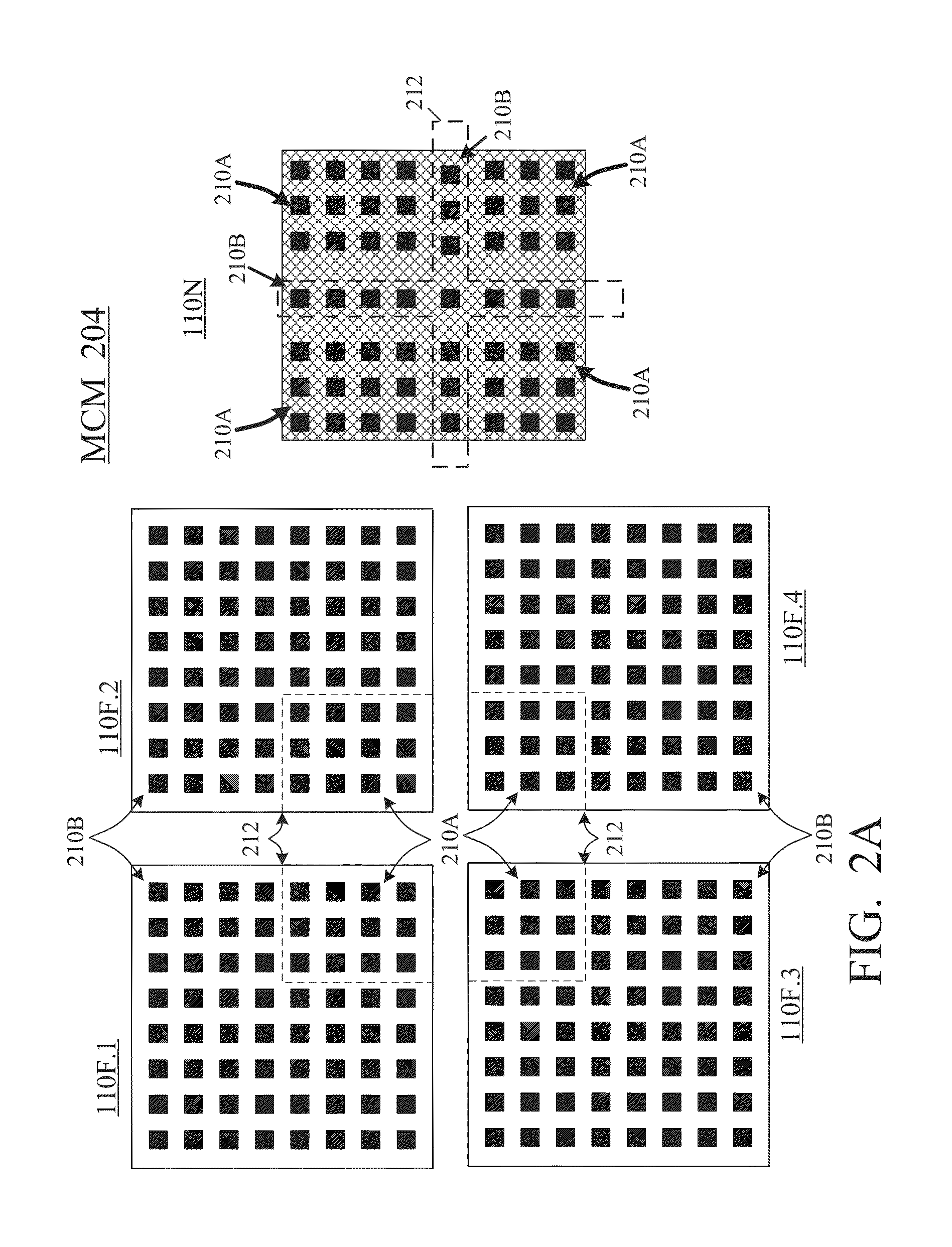
[0041]FIGS. 2A and 2B illustrate an exemplary multi-chip module (MCM) 204 with four plain chips 110F.1, 110F.2, 110F.3, 110F.4 interconnected by a super chip 110N. Plain chips 110F (i.e. 110F.1 through 110F.4) and super chip 110N can be any chips 110 shown in FIG. 1 or any other chips. In a non-limiting example, chip 110F.1 is a CPU (like 110F.1 in FIG. 1), chip 110F.2 is a GPU (like 110F.7 in FIG. 1), chip 110F.3 is a RAM (like 110F.10 in FIG. 1), and chip 110F.4 is a PMIC (like 110F.4 in FIG. 1). The plain chips' IOs 210 include high-speed IOs 210A and low-speed IOs 210B. We refer to high-speed IOs 210A as “group A”, and to low-speed IOs 210B as “group B”. Each group may include only one IO or multiple IOs.

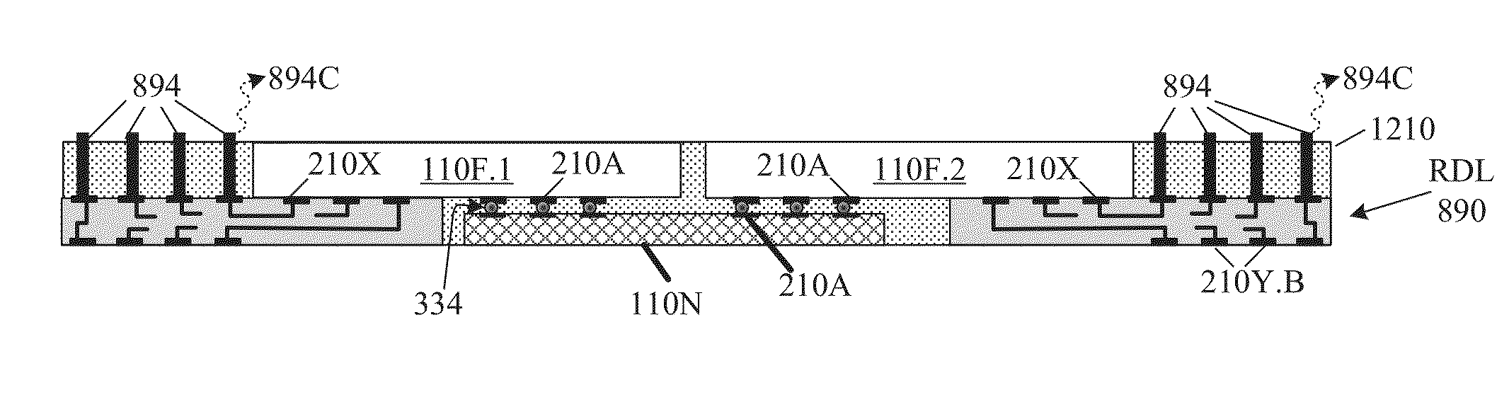
[0042]Super chip 110N has IOs 210A attached to plain chips 110F, and IOs 210B in the middle that will be directly connected to a (possibly coarse) WB.

[0043]FIG. 2A illustrates each chip sep...


PUM

PropertyMeasurementUnit
Timeaaaaaaaaaa
Thicknessaaaaaaaaaa
Electrical conductoraaaaaaaaaa

Abstract

In a multi-chip module (MCM), a “super” chip (110N) is attached to multiple “plain” chips (110F′“super” and “plain” chips can be any chips). The super chip is positioned above the wiring board (WB) but below at least some of plain chips (110F). The plain chips overlap the super chip. Further, the plain chips' low speed IOs can be connected to the WB by long direct connections such as bond wires (e.g. BVAs) or solder stacks; such connections can be placed side by side with the super chip. Such connections can be long, so the super chip is not required to be thin. Also, if through-substrate vias (TSVs) are omitted, the manufacturing yield is high and the manufacturing cost is low. Other structures are provided that combine the short and long direct connections to obtain desired physical and electrical properties.

Description

CROSS-REFERENCE TO RELATED APPLICATIONS[0001]The present application claims priority of U.S. provisional patent application No. 62 / 046,395, filed 5 Sep. 2014, incorporated herein by reference.BACKGROUND OF THE INVENTION[0002]The present invention relates to integrated circuits, and more particularly to multi-chip modules (MCMs).[0003]The following documents relate to integrated circuits and may be of background interest:[0004]U.S. pre-grant patent publication 2009 / 0267238 (Oct. 29, 2009; Joseph et al.).[0005]U.S. pre-grant patent publication 2012 / 0020027 (Jan. 26, 2012, Dungan et al.)[0006]A multi-chip module (MCM) is an assembly of multiple components, with one or more components being integrated circuits (ICs), such that the assembly can be used like a single semiconductor integrated circuit. A usual (not multi-chip) semiconductor integrated circuit can be manufactured as a wafer or as a die (single-chip IC) formed in a wafer and later separated from the wafer (when the wafer is d...

Claims


Application Information

Patent Timeline
IPC IPC(8): H01L25/065B81B7/00B81C1/00H01L21/56H01L21/768H01L23/00H01L23/31H01L23/367H01L23/48H01L23/498H01L23/538H01L25/00H01L25/18
CPCH01L25/0652H01L2224/80001H01L24/06H01L23/367H01L24/49H01L25/18B81B7/008H01L23/5389H01L21/565H01L25/50H01L23/481H01L21/76877B81C1/0023H01L23/3107H01L24/89B81B2207/07H01L2224/04042H01L2224/08225H01L2224/06181H01L2224/48137H01L2225/06506H01L2225/06527H01L2225/06548H01L2225/06589H01L2924/1461H01L2924/14H01L2924/1511H01L23/49838H01L24/19H01L24/20H01L24/96H01L25/0655H01L25/0657H01L25/10H01L25/105H01L2224/12105H01L2224/0401H01L2224/04105H01L2224/16145H01L2224/32225H01L2224/45015H01L2224/45099H01L2224/73257H01L2224/73253H01L2224/73265H01L2224/73204H01L2224/73209H01L2224/73207H01L2224/48227H01L2224/81005H01L2924/00012H01L2924/00014H01L2224/92124H01L2224/92133H01L2225/0651H01L2225/06513H01L2225/06517H01L2924/15153H01L2924/15192H01L2924/207H01L2924/18162H01L2924/18161H01L24/48H01L2924/3511H01L2224/73104H01L2224/05599H01L2224/85399H01L23/3157H01L23/34H01L24/09H01L24/17H01L24/33H01L2224/09181H01L2224/33517H01L2224/48135H01L2924/01029H01L2924/014H01L2924/07802
Inventor WANG, LIANGKATKAR, RAJESHSHEN, HONG
Owner INVENSAS LLC
Why Eureka
Try Eureka