Substrate processing apparatus, method of manufacturing semiconductor device and furnace lid

a technology of semiconductor devices and processing equipment, which is applied in the direction of lighting and heating equipment, furnace types, furnaces, etc., can solve the problems of difficult to heat the low-temperature region of the heating unit, and achieve the effect of reducing the risk of heat loss

Inactive Publication Date: 2016-03-17
KOKUSA ELECTRIC CO LTD
View PDF3 Cites 44 Cited by
  • Summary
  • Abstract
  • Description
  • Claims
  • Application Information

AI Technical Summary

Benefits of technology

[0006]However, in the substrate processing apparatus, a low-temperature region which is difficult for the heating unit to heat may be generated in the reaction tube.

Problems solved by technology

However, in the substrate processing apparatus, a low-temperature region which

Method used


Image

  • Substrate processing apparatus, method of manufacturing semiconductor device and furnace lid
  • Substrate processing apparatus, method of manufacturing semiconductor device and furnace lid
  • Substrate processing apparatus, method of manufacturing semiconductor device and furnace lid

Examples


Embodiment Construction

An Embodiment of the Present Invention

[0024]Hereinafter, an embodiment of the present invention will be described with reference to the drawings.

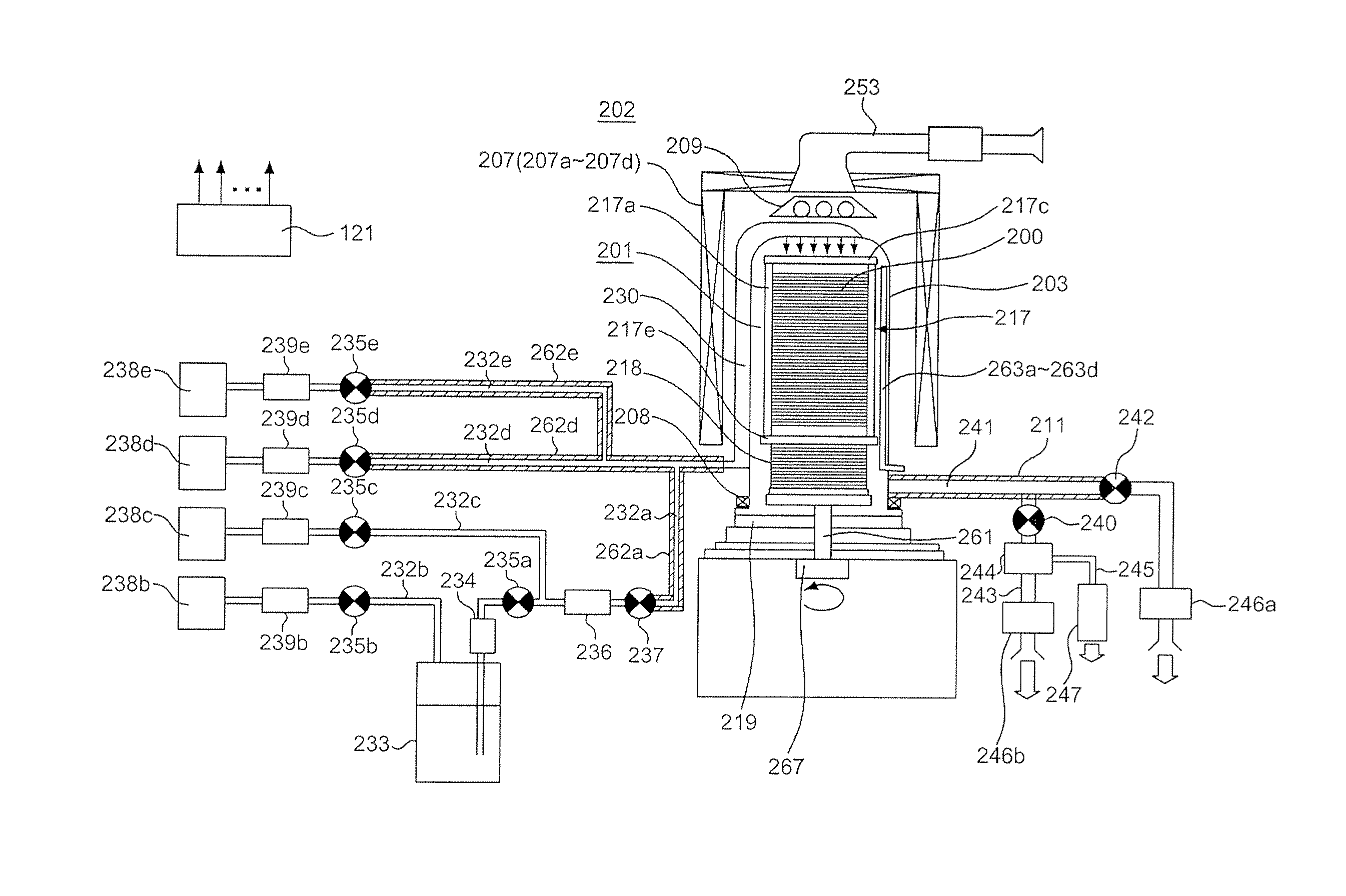
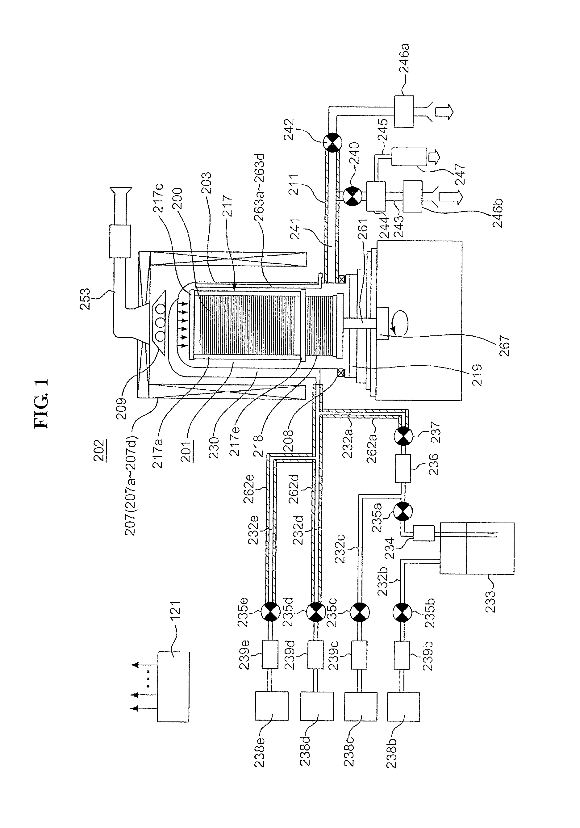
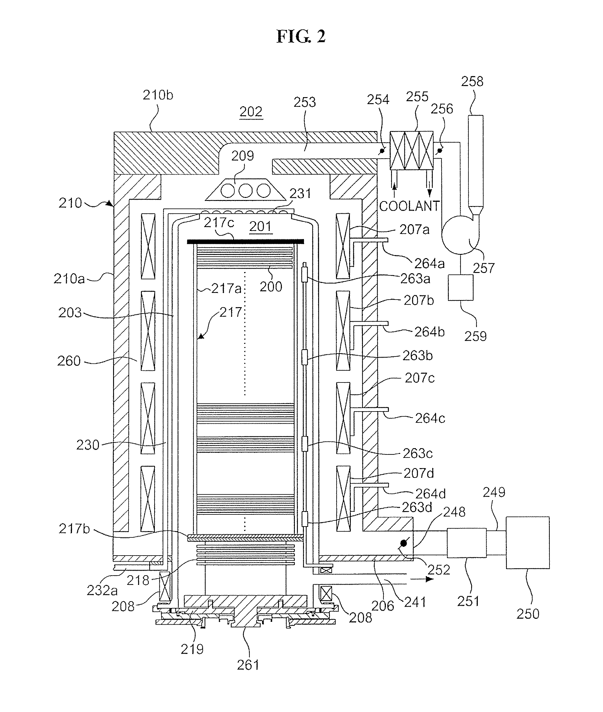
[0025](1) Configuration of Substrate Processing Apparatus

[0026]First, a configuration of a substrate processing apparatus according to the present embodiment will be mainly described with reference to FIGS. 1 and 2. FIG. 1 is a cross-sectional view schematically illustrating the substrate processing apparatus according to the present embodiment and is a longitudinal cross-sectional view illustrating a treatment furnace 202. FIG. 2 is a longitudinal cross-sectional view schematically illustrating the treatment furnace 202 included in the substrate processing apparatus according to the present embodiment.

[0027](Reaction Tube)

[0028]Referring to FIG. 1, the treatment furnace 202 includes a reaction tube 203. The reaction tube 203 is made of, for example, a heat-resistant material such as quartz (SiO2) or silicon carbide (SiC), and is formed in ...


PUM

PropertyMeasurementUnit
Temperatureaaaaaaaaaa
Heataaaaaaaaaa
Perimeteraaaaaaaaaa

Abstract

By suppressing a re-liquefaction of a processing gas in a reaction tube, the processing gas is maintained in a gaseous state. There is provided a substrate processing apparatus that includes a reaction tube, a supply unit, an exhaust unit, a first heating unit configured to heat a substrate in the reaction tube, a second heating unit configured to heat a downstream portion of a reactant in gaseous state flowing in the reaction tube from the supply unit toward the exhaust unit, and a furnace lid, wherein the furnace lid includes a heat absorbing unit facing a lower surface of a lower end portion of the reaction tube and being heated by the second heating unit, the heat absorbing unit having an outer perimeter surface disposed outer than an inner circumference surface of the lower end portion.

Description

CROSS-REFERENCE TO RELATED PATENT APPLICATION[0001]This non-provisional U.S. patent application claims priority under 35 U.S.C. §119 of Japanese Patent Application No. 2013-116106, filed on May 31, 2013, and PCT / JP2014 / 064263, filed on May 29, 2014, the entire contents of which are hereby incorporated by reference.BACKGROUND OF THE INVENTION[0002]1. Field of the Invention[0003]The present invention relates to a substrate processing apparatus, a method of manufacturing a semiconductor device and a furnace lid.[0004]2. Description of the Related Art[0005]Conventionally, as one of processes of manufacturing a semiconductor device such as a dynamic random access memory (DRAM) or the like, a process in which a processing gas is supplied into a reaction tube in which a substrate is loaded to form an oxide film on a surface of the substrate may be performed. Such a process is performed by a substrate processing apparatus that includes, for example, a reaction tube configured to accommodate...

Claims


Application Information

Patent Timeline
IPC IPC(8): C23C16/52C23C16/44C23C16/455C23C16/46F27D1/18H01L21/02
CPCC23C16/52C23C16/46F27D1/1816C23C16/455H01L21/02271C23C16/4412C23C16/4401F27B17/0025H01L21/02238H01L21/02255H01L21/02304H01L21/32105
Inventor YAMAZAKI, KEISHINIZUMI, MANABUNOGAMI, KATSUAKI
Owner KOKUSA ELECTRIC CO LTD
Why Eureka
Try Eureka