Inspection Apparatus And Device Manufacturing Method

a technology of inspection apparatus and manufacturing method, which is applied in the direction of measurement devices, material analysis, instruments, etc., can solve the problems of layout difficulties, devices that have not been implemented for inspection lights, and are sensitive to vibration and wear, so as to improve measurement speed and/or measurement performance, and improve radiation utilization

Active Publication Date: 2016-03-31
ASML NETHERLANDS BV
View PDF20 Cites 35 Cited by
  • Summary
  • Abstract
  • Description
  • Claims
  • Application Information

AI Technical Summary

Benefits of technology

[0011]The present invention aims to provide alternative illumination systems for metrology and other applications in which an illumination profile can be selected by a programmable device, without some of the compromises that would otherwise result. For example, the invention may improve utilization of radiation to allow improved measurement speed and / or measurement performance.

Problems solved by technology

There are several moving parts in the known illumination system, making it sensitive to vibrations and wear.
However, in practice these devices have not been implemented for the illuminator.
One reason for this may be that providing reflective programmable SLMs such as DMDs in the illumination path requires convoluted beam paths and cause layout difficulties.
A problem with LC shutter type devices is that they generally deliver only one polarization of light, while metrology applications require freedom to control polarization as an illumination parameter in the recipe.
A problem in known designs is that one or more beam splitting elements are normally used to deliver and / or collect the inspection radiation.
Up to half of the available radiation may be lost at each beam splitter.
Therefore measurements are taken with low light intensity, from which it is difficult to obtain low-noise measurements with high throughput.
Liquid crystal-type SLMs additionally block at least half of the usable light, adding to this difficulty.

Method used


Image

  • Inspection Apparatus And Device Manufacturing Method
  • Inspection Apparatus And Device Manufacturing Method
  • Inspection Apparatus And Device Manufacturing Method

Examples


application example

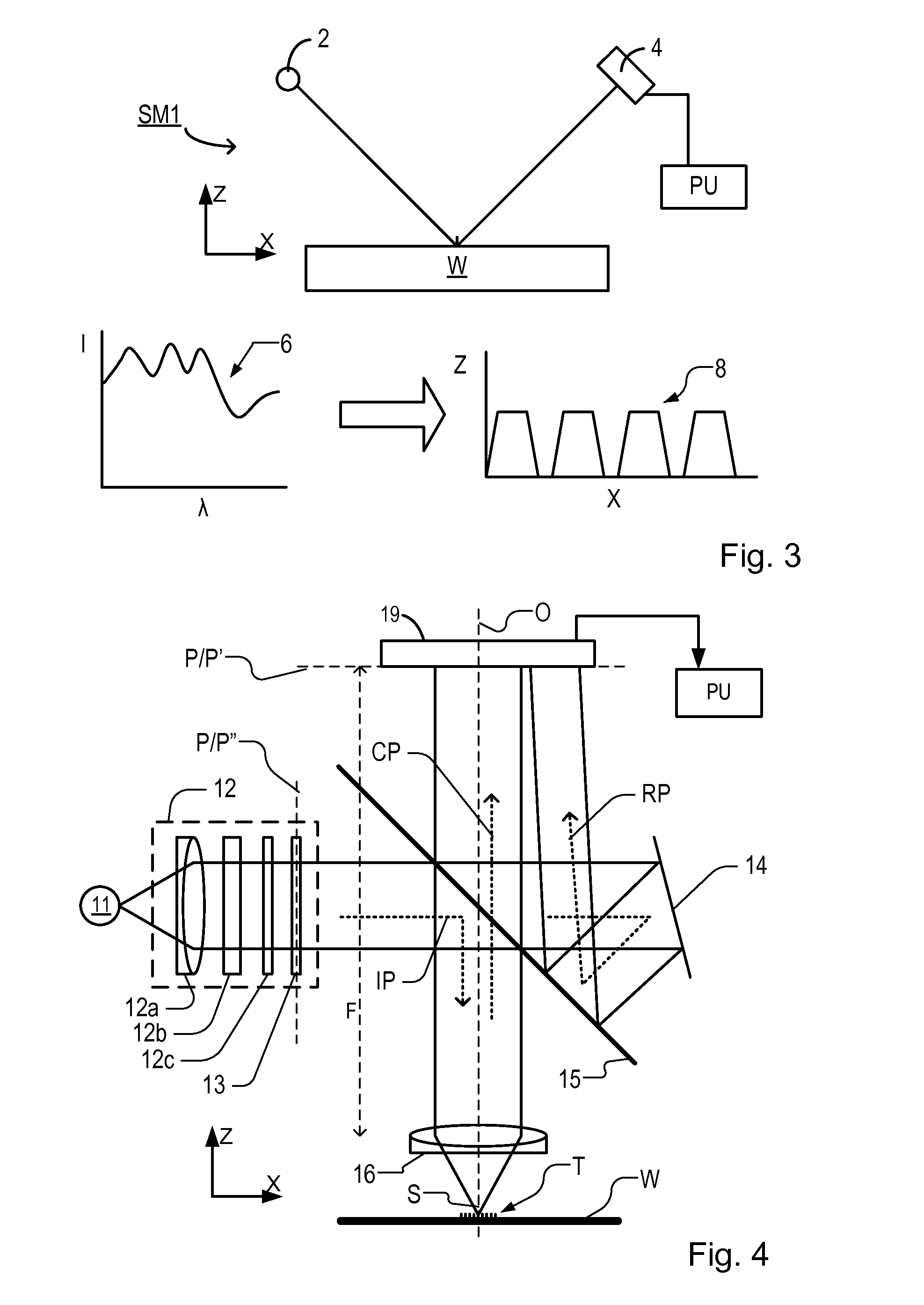
[0111]FIG. 12 is a flowchart showing the application of the inspection apparatus of the above embodiments in monitoring and control of a lithographic process in the manufacture of devices. In step S1 a substrate W is loaded into the inspection apparatus. The substrate has one or more target structures that have been formed by the lithographic process. A target T is located in the field of view of the optical system, for example beneath objective lens 16. In step S2, the mirror array device 713 is set into desired configuration, with different mirror elements being positioned to define active areas of the illumination path IP and collection path CP. Optionally, of course, configurations having third positions may be implemented, as discussed above.

[0112]In step S3, the inspection apparatus is operated to capture scattered radiation using the defined configuration. Referring to the example of FIG. 10, optional steps S4 and S5 may be performed to capture images using a reversed configu...


PUM

PropertyMeasurementUnit
wavelengthsaaaaaaaaaa
angle θ2aaaaaaaaaa

Abstract

An inspection apparatus comprises an illumination system (12) for illuminating a target structure with illuminating radiation and a collection system for collecting the illuminating radiation after it has been scattered by the target structure. A programmable spatial light modulator (713) comprises an array of movable mirror elements (742) in a conjugate pupil plane (P″) of the illumination system. Between the array of mirror elements and the target a common optical path is defined forming part of the illumination system and the collection system. Each mirror element is movable between a first position where it reflects illuminating radiation into the common optical path and a second position where it reflects radiation from the common optical path toward a detector (19, 23). Various combinations of illumination aperture and collection aperture can be defined without the light losses associated with beam splitters and transmissive spatial light modulators.

Description

BACKGROUND[0001]1. Field of the Invention[0002]The present invention relates to inspection apparatus and methods usable, for example, to perform metrology in the manufacture of devices by lithographic techniques. The invention further relates to methods of manufacturing devices using lithographic techniques.[0003]2. Background Art[0004]A lithographic apparatus is a machine that applies a desired pattern onto a substrate, usually onto a target portion of the substrate. A lithographic apparatus can be used, for example, in the manufacture of integrated circuits (ICs). In that instance, a patterning device, which is alternatively referred to as a mask or a reticle, may be used to generate a circuit pattern to be formed on an individual layer of the IC. This pattern can be transferred onto a target portion (e.g., including part of, one, or several dies) on a substrate (e.g., a silicon wafer). Transfer of the pattern is typically via imaging onto a layer of radiation-sensitive material (...

Claims


Application Information

Patent Timeline
Patent Type & Authority Applications(United States)
IPC IPC(8): G01N21/47
CPCG01N21/4738G01N2201/0636G01N2201/061G01N2201/12G01N21/956G01N2021/95676G03F7/70625G03F7/70633
Inventor VAN, DER, ZOUW, GERBRAND
Owner ASML NETHERLANDS BV
Why Eureka
Try Eureka