
Dynamic random access memory timing adjustments

a random access memory and timing adjustment technology, applied in the field of dynamic random access memories, can solve the problems of data errors at the dram, timing margin violation at the latch coupled to the data receiver, increased jitter between the data receiver and the clock receiver, etc., to reduce the amount of voltage drift, reduce the data rate of data traffic, and reduce the effect of voltage fluctuations

Inactive Publication Date: 2016-03-31
QUALCOMM INC
View PDF4 Cites 1 Cited by
  • Summary
  • Abstract
  • Description
  • Claims
  • Application Information

AI Technical Summary

Benefits of technology

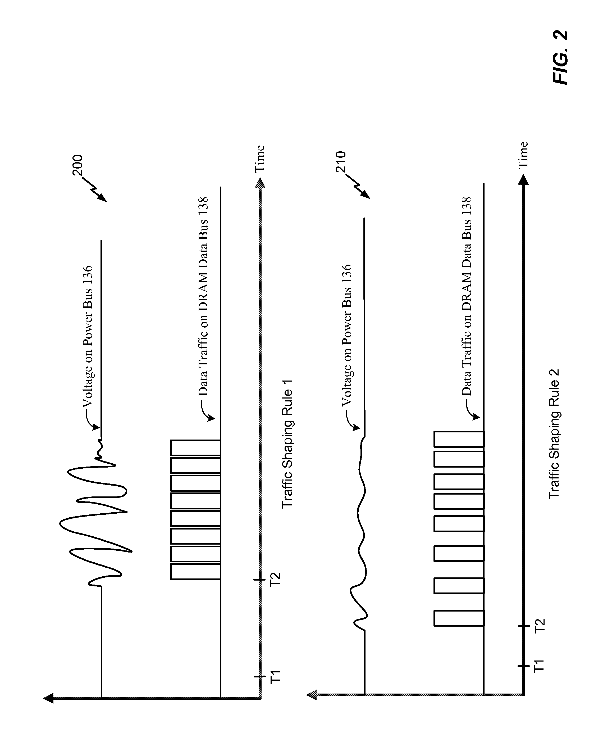
The patent describes a technology that reduces the fluctuations in voltage at the power bus of a computer chip. This is done by slowing down the data traffic on the chip's data bus when there is a sudden increase in the amount of data being sent. This reduction of noise decreases the amount of "jitter" between the chip's data receiver and clock receiver, improving the overall performance of the chip.

Problems solved by technology

When a timing margin is violated (e.g., when data is sent and / or received during non-transition periods of a clock cycle), data errors may occur at the DRAM.
Voltage drift (e.g., voltage fluctuations) on the power bus may cause jitter (e.g., a timing offset or a timing margin violation) at latches coupled to the data receiver and the clock receiver.
However, as the frequency of operation increases and the timing margin decreases, voltage drift on the power bus may cause an increased amount of jitter between the data receiver and the clock receiver.
However, sending a burst of data (e.g., a relatively large amount of data in a short time period) to the data receiver via a DRAM data bus after an idle period (e.g., a period of time when data is not sent via the DRAM data bus) may cause voltage fluctuations (e.g., noise) on the power bus.
The voltage fluctuations on the power bus may cause timing skew (e.g., jitter or a timing violation) between the data receiver and the clock receiver.
For example, sending a burst of data to the data receiver may require that the power source provide an increased amount of power to the controller during a short period of time, which may cause voltage fluctuations on the power bus.

Method used


Image

  • Dynamic random access memory timing adjustments
  • Dynamic random access memory timing adjustments
  • Dynamic random access memory timing adjustments

Examples


Embodiment Construction

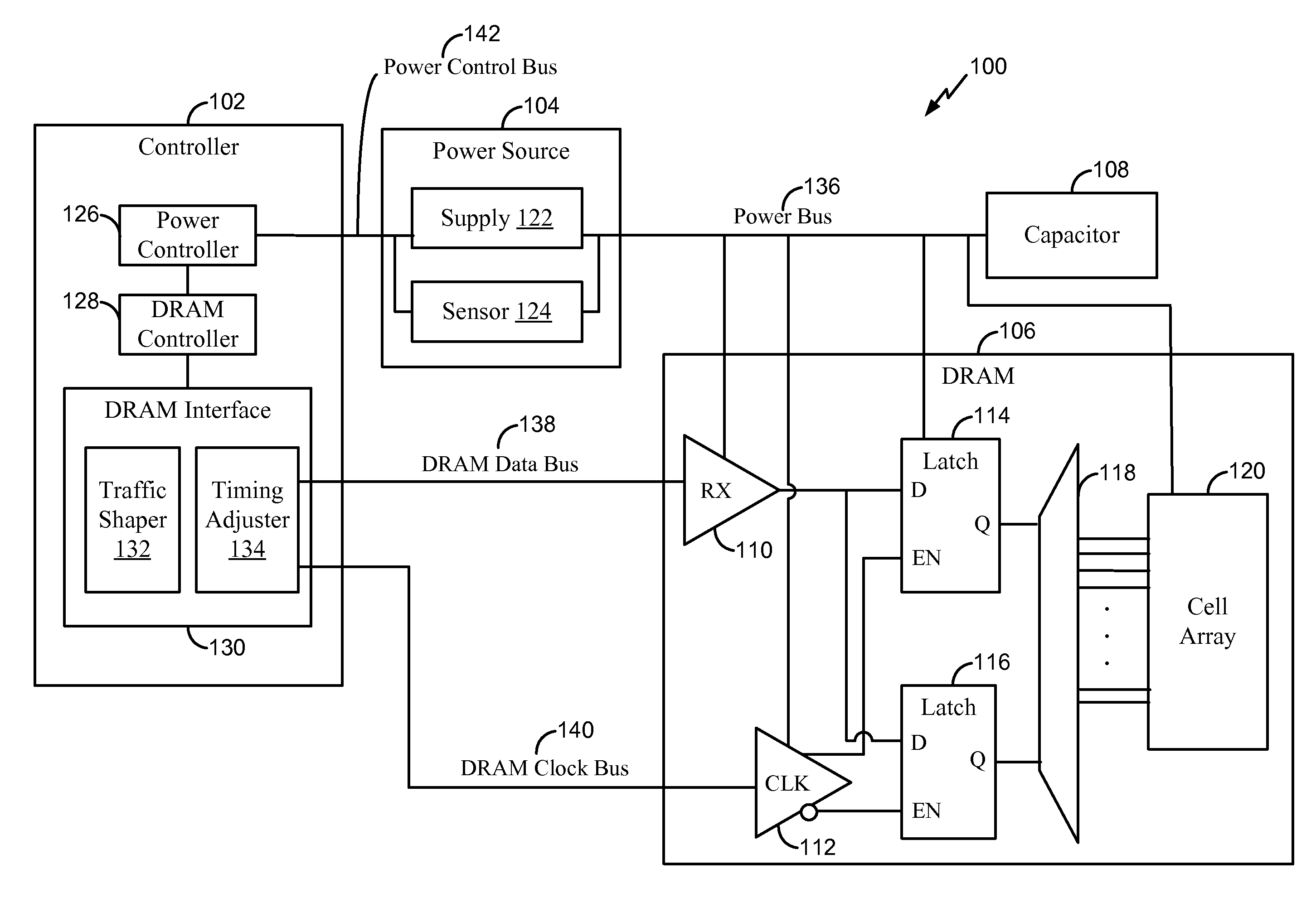
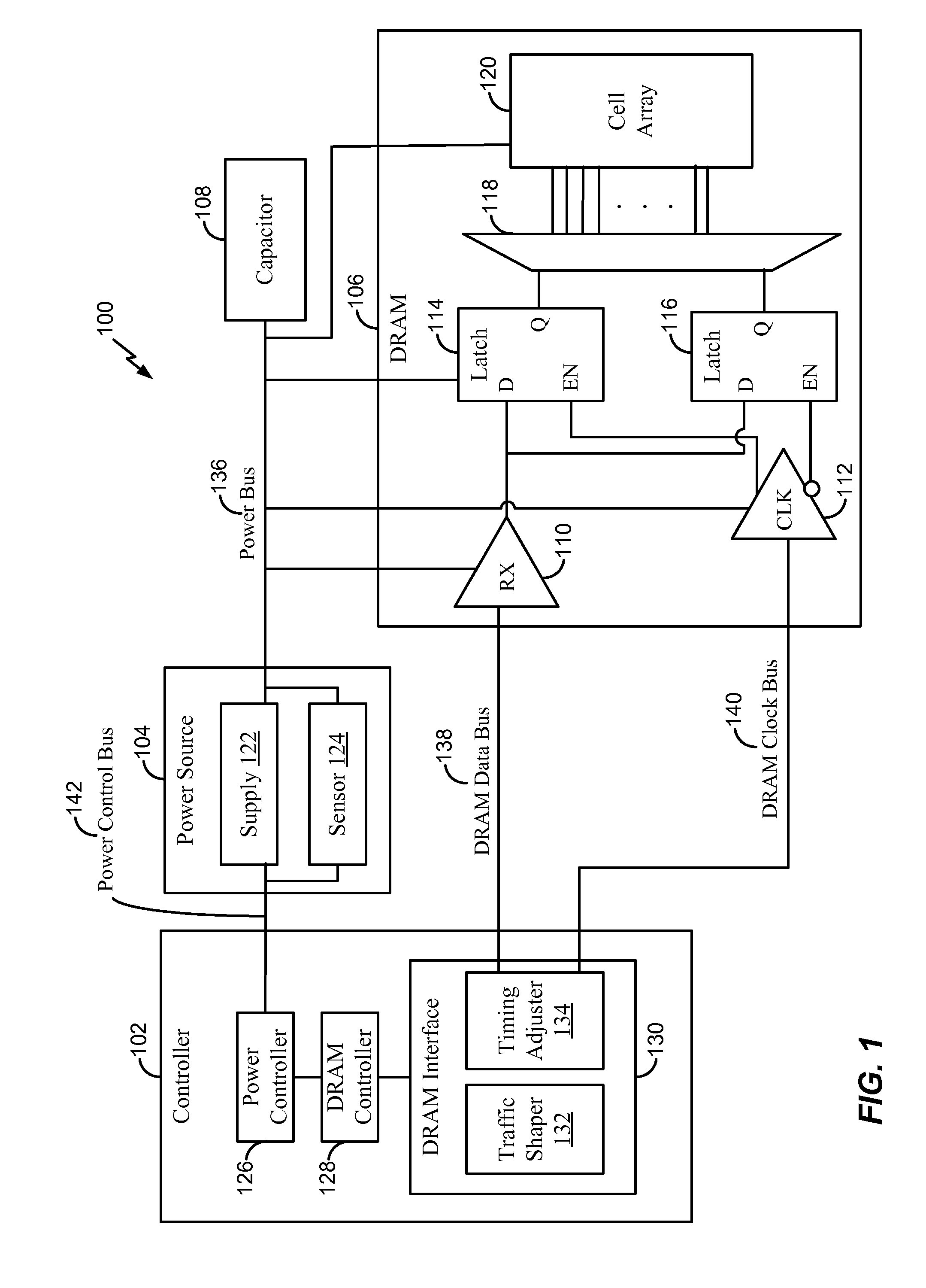
[0026]Referring to FIG. 1, a particular illustrative aspect of a system 100 that is operable to reduce jitter-based errors at a dynamic random access memory (DRAM) is shown. The system 100 includes a controller 102, a power source 104, a DRAM 106, and a capacitor 108.

[0027]The DRAM 106 includes a data receiver (RX) 110 and a clock receiver (CLK) 112. The data receiver 110 and the clock receiver 112 may be coupled to receive power from a power bus 136. The DRAM 106 also includes a first latch 114 (e.g., a first D-type flip-flop circuit) and a second latch 116 (e.g., a second D-type flip-flop circuit). For example, an output of the data receiver 110 may be coupled to a data input (D) of the first latch 114 and to a data input (D) of the second latch 116. An output of the clock receiver 112 may be coupled to an enable input (EN) of the first latch 114, and an inverted output of the clock receiver 112 may be coupled to an enable input (EN) of the second latch 116. For example, the clock...


PUM


Abstract

A method includes detecting, at a controller, a rate-of-change between first data traffic to be sent to a dynamic random access memory (DRAM) at a first time and second data traffic to be sent to the DRAM at a second time. The method also includes adjusting a data rate of the second data traffic in response to a determination that the rate-of-change satisfies a threshold.

Description

I. FIELD[0001]The present disclosure is generally related to dynamic random access memories (DRAMs).II. DESCRIPTION OF RELATED ART[0002]Advances in technology have resulted in smaller and more powerful computing devices. For example, a variety of portable personal computing devices including wireless telephones, such as mobile and smart phones, tablets, and laptop computers, are small, lightweight, and easily carried by users. These devices can communicate voice and data packets over wireless networks. Further, many such devices incorporate additional functionalities such as a digital still camera, a digital video camera, a digital recorder, and an audio file player. Also, such devices can process executable instructions, including software applications, such as a web browser application, that can be used to access the Internet. As such, these devices can include significant computing capabilities.[0003]Electronic devices may include a dynamic random access memory (DRAM) to store da...

Claims


Application Information

Patent Timeline
Patent Type & Authority Applications(United States)
IPC IPC(8): G11C7/10
CPCG11C7/1072G06F13/1689
Inventor CHUN, DEXTER, TAMIODROP, MICHAELSANKURATRI, RAGHU
Owner QUALCOMM INC
Learn More