Semiconductor manufacturing equipment component and method of making the same

a manufacturing equipment and semiconductor technology, applied in the field of semiconductor manufacturing equipment components and semiconductor manufacturing equipment components, can solve the problems of reducing the processing precision of semiconductor wafers, affecting the quality of semiconductor wafers, and difficult for heating elements to generate heat uniformly, so as to suppress the temperature variation of the body substrate and suppress the thickness and width of the heating elemen

Inactive Publication Date: 2016-04-07
NGK SPARK PLUG CO LTD
View PDF6 Cites 6 Cited by
  • Summary
  • Abstract
  • Description
  • Claims
  • Application Information

AI Technical Summary

Benefits of technology

[0009]The present invention, which has been made against the aforementioned background, provides a semiconductor manufacturing equipment component in which variations in the thickness and the width of a heating element are suppressed and that can suppress temperature variation of a body substrate in which the heating element is disposed and a method of making the semiconductor manufacturing equipment component.
[0012]Thus, in the firing step, it is possible to form the heating element in which variations in thickness and width are suppressed and that can generate heat uniformly. Thus, temperature variation (temperature variation in the in-plane direction) of the body substrate, in which the heating element is disposed, can be suppressed. Moreover, temperature variation of the semiconductor wafer or the like, which is supported by the body substrate, can be suppressed. As a result, for example, the precision in etching the semiconductor wafer can be increased, and the yield can be improved.
[0013]Moreover, even if the pattern of the intermediate heating element (the heating element material), which is formed by using photolithography, includes lines having different line widths, variations in the thickness and the width of the pattern can be suppressed. Thus, for example, a heating element having a complex pattern including lines having different line widths can be formed with high precision.
[0017]In the semiconductor manufacturing equipment component, the heating element, which is disposed in the body substrate, has a rectangular cross section. Therefore, variations in the thickness and the width of the heating element are small, and the heating element can generate heat uniformly. Thus, temperature variation (temperature variation in the in-plane direction) of the body substrate, in which the heating element is disposed, can be suppressed. Moreover, temperature variation of the semiconductor wafer or the like, which is supported by the body substrate, can be suppressed. As a result, for example, the precision in etching the semiconductor wafer can be increased, and the yield can be improved.
[0018]As described above, with the present invention, it is possible to provide a semiconductor manufacturing equipment component in which variations in the thickness and the width of a heating element are suppressed and that can suppress temperature variation of a body substrate in which the heating element is disposed and a method of making the semiconductor manufacturing equipment component.
[0027]The body substrate may include, for example, a stack of ceramic layers. With such a structure, various structures (such as the heating element and the like) can be easily formed in the body substrate.

Problems solved by technology

However, the electrostatic chuck described in Japanese Unexamined Patent Application Publication No. 2004-71647 has the following problem.
When screen printing is used, however, print staining, mesh marking of a screen mask, displacement of the screen mask, difference between the print direction and the patterning direction, and the like may occur.
Therefore, the thickness and the width of the heating element after being fired may vary, and it is difficult for the heating element to generate heat uniformly.
As a result, the processing precision of the semiconductor wafer may decrease.

Method used


Image

  • Semiconductor manufacturing equipment component and method of making the same
  • Semiconductor manufacturing equipment component and method of making the same
  • Semiconductor manufacturing equipment component and method of making the same

Examples


first embodiment

A. First Embodiment

[0050]The present embodiment is an example in which a semiconductor manufacturing equipment component according to the present invention is applied to an electrostatic chuck.

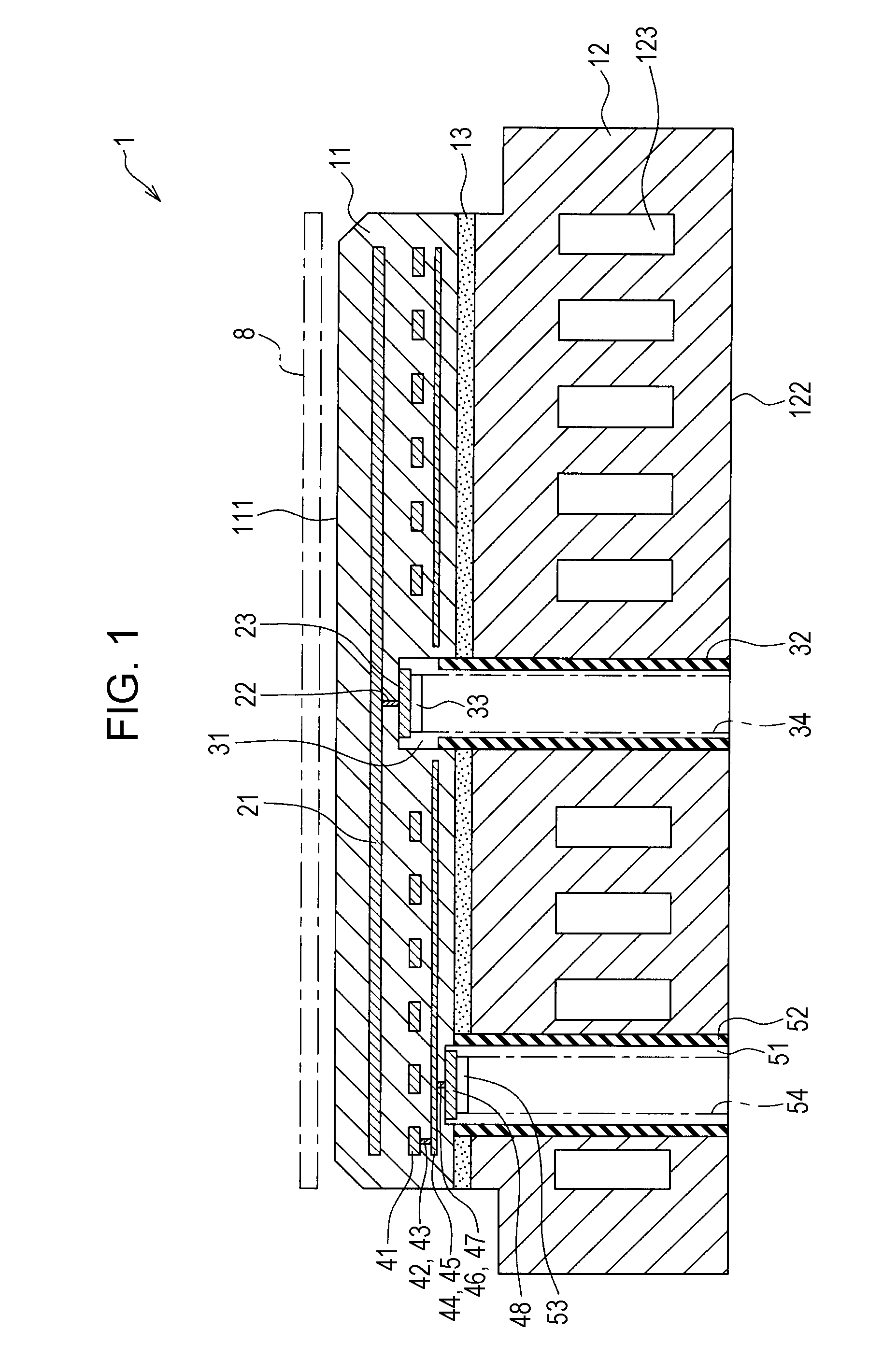
[0051]Referring to FIGS. 1 to 3D, an electrostatic chuck 1 (semiconductor manufacturing equipment component) includes a body substrate 11 made of a ceramic and a heating element 41 disposed in the body substrate 11. The heating element 41 has a rectangular cross section. Hereinafter, the electrostatic chuck 1 will be described in detail.

[0052]Referring to FIG. 1, the electrostatic chuck 1 attracts and holds a semiconductor wafer 8, which is an object to be held. The electrostatic chuck 1 includes the body substrate 11, a metal base 12, and an adhesive layer 13. The body substrate 11 and the metal base 12 are joined to each other through the adhesive layer 13 disposed therebetween.

[0053]In the present embodiment, the body substrate 11 is disposed above the metal base 12 in the vertical directio...

second embodiment

B. Second Embodiment

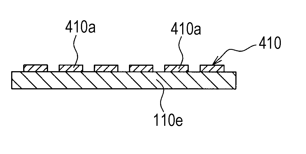
[0094]FIGS. 8A to 9B illustrate a second embodiment, which is a modified example of the method of making the electrostatic chuck 1 (see FIGS. 1 to 3D) according to the first embodiment described above.

[0095]Referring to FIGS. 8A to 9B, the method of making the electrostatic chuck 1 (semiconductor manufacturing equipment component) according to the present embodiment includes an application step of applying the photosensitive metal paste 410 onto a carrier film 600, the photosensitive metal paste 410 being a heating element material; an exposure-and-development step of exposing the photosensitive metal paste 410, which has been applied onto the carrier film 600, to light and developing the photosensitive metal paste 410 to form the intermediate heating element 410a, which is to become the heating element 41, on the carrier film 600; a transfer step of transferring the intermediate heating element 410a on the carrier film 600 onto a ceramic green sheet 110e, which ...

example

[0106]In the present example, variations of the surface roughness and the thickness of heating element materials patterned by using different methods were evaluated. The shapes of heating elements obtained by co-firing the heating element materials, which were patterned by using different methods, and the ceramic green sheet were observed.

[0107]First, by using a photosensitive metal paste (heating element material) the same as that of the first embodiment, a pattern was formed on a ceramic green sheet (alumina green sheet) by photolithography in the same way as in the first embodiment (sample 11). For comparison, by using an existing metal paste (heating element material), a pattern was formed on a ceramic green sheet by screen printing (sample 21). In each of the samples 11 and 21, the line width was 0.70 mm.

[0108]Next, by using a contact profilometer (SURFCOM 1500SD3, made by Tokyo Seimitsu Co., Ltd.), the surface roughnesses of the heating element materials of the samples 11 and ...


PUM

PropertyMeasurementUnit
surface roughness Raaaaaaaaaaa
widthaaaaaaaaaa
widthaaaaaaaaaa

Abstract

A method of making a semiconductor manufacturing equipment component, such as an electrostatic chuck, includes an application step of applying a photosensitive metal paste onto a ceramic green sheet, which is to become the body substrate, the photosensitive metal paste being a heating element material; an exposure-and-development step of exposing the photosensitive metal paste, which has been applied onto the ceramic green sheet, to light and developing the photosensitive metal paste to form an intermediate heating element, which is to become the heating element, on the ceramic green sheet; and a firing step of co-firing the ceramic green sheet and the intermediate heating element to form the body substrate and the heating element.

Description

CROSS REFERENCE TO RELATED APPLICATIONS[0001]The present application claims priority to Japanese Patent Application No. 2014-203305, which was filed on Oct. 1, 2014, the disclosure of which is herein incorporated by reference in its entirety.BACKGROUND OF THE INVENTION[0002]1. Field of the Invention[0003]The present invention relates to a semiconductor manufacturing equipment component and a method of making a semiconductor manufacturing equipment component.[0004]2. Description of the Related Art[0005]Existing semiconductor manufacturing equipment performs dry etching (such as plasma etching) or other processing of a semiconductor wafer (such as a silicon wafer). To increase the processing precision, it is necessary that the semiconductor manufacturing equipment have supporting means that can reliably support the semiconductor wafer in the equipment. An electrostatic chuck, which supports a semiconductor wafer by using an electrostatic attraction force, is known as the supporting me...

Claims


Application Information

Patent Timeline
Patent Type & Authority Applications(United States)
IPC IPC(8): H01L21/683B32B37/00G03F7/40H01L21/687
CPCH01L21/6833H01L21/68757B32B37/025G03F7/40B32B2457/00B32B2315/02B32B2311/00B32B2398/00B32B2310/0806G03F7/00G03F7/20H01L21/67103H01L21/6831B32B18/00B32B2457/14C04B37/021C04B37/028C04B2237/127C04B2237/343C04B2237/402C04B2237/62C04B2237/64C04B2237/66C04B2237/706
Inventor NASU, TAKAKUNINIWA, TOMONORIKIBE, TAICHI
Owner NGK SPARK PLUG CO LTD
Why Eureka
Try Eureka