Semiconductor device, imaging device, and electronic device

a technology of electromagnetic field and electromagnetic field, applied in the direction of radio frequency controlled devices, transistors, television systems, etc., can solve the problems of reducing aperture ratio and increasing pixel area, and achieve the effect of reducing power consumption and reducing area

Inactive Publication Date: 2016-05-05
SEMICON ENERGY LAB CO LTD
View PDF10 Cites 14 Cited by
  • Summary
  • Abstract
  • Description
  • Claims
  • Application Information

AI Technical Summary

Benefits of technology

[0021]According to one embodiment of the present invention, a novel semiconductor device, a semiconductor device with reduced area, a versatile semiconductor device, a sem

Problems solved by technology

However, in the case where different power source lines are provided for the amplifier and the reset transistor, space for two p

Method used


Image

  • Semiconductor device, imaging device, and electronic device
  • Semiconductor device, imaging device, and electronic device
  • Semiconductor device, imaging device, and electronic device

Examples


embodiment 1

[0054]In this embodiment, a structure example of a semiconductor device of one embodiment of the present invention is described.

10>

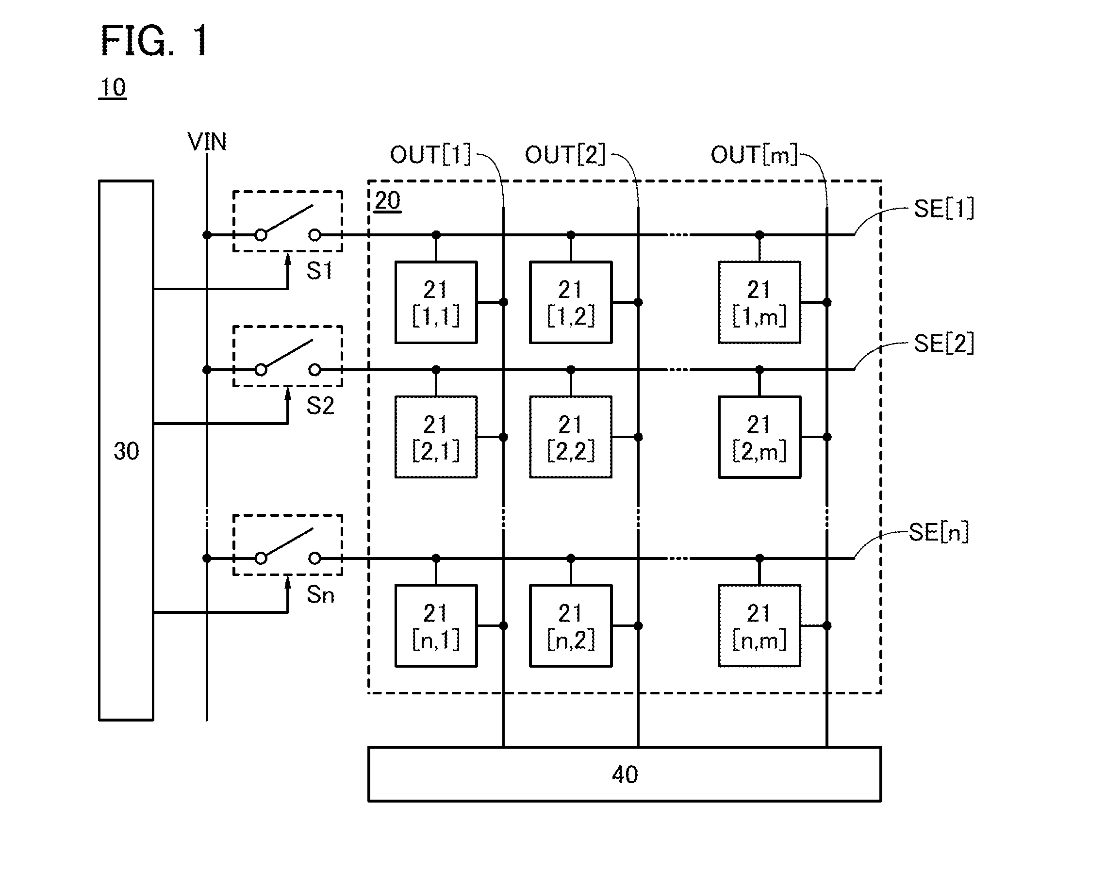
[0055]FIG. 1 illustrates a structure example of a semiconductor device 10 of one embodiment of the present invention. The semiconductor device 10 includes a pixel portion 20, a circuit 30, and a circuit 40. The semiconductor device 10 further includes a wiring VIN and a plurality of switches S outside the pixel portion 20.

[0056]The pixel portion 20 includes a plurality of pixels 21. Shown here is an example in which the pixels 21[1,1] to 21[n,m] are provided in n rows and m columns (n and m are natural numbers) in the pixel portion 20. Each pixel 21 has a function of converting irradiation light into an electrical signal (hereinafter also referred to as an optical data signal). Each pixel 21 thus serves as a photodetector circuit in an imaging device. Specifically, irradiation light of a photoelectric conversion element provided in each pixel 21 is conve...

embodiment 2

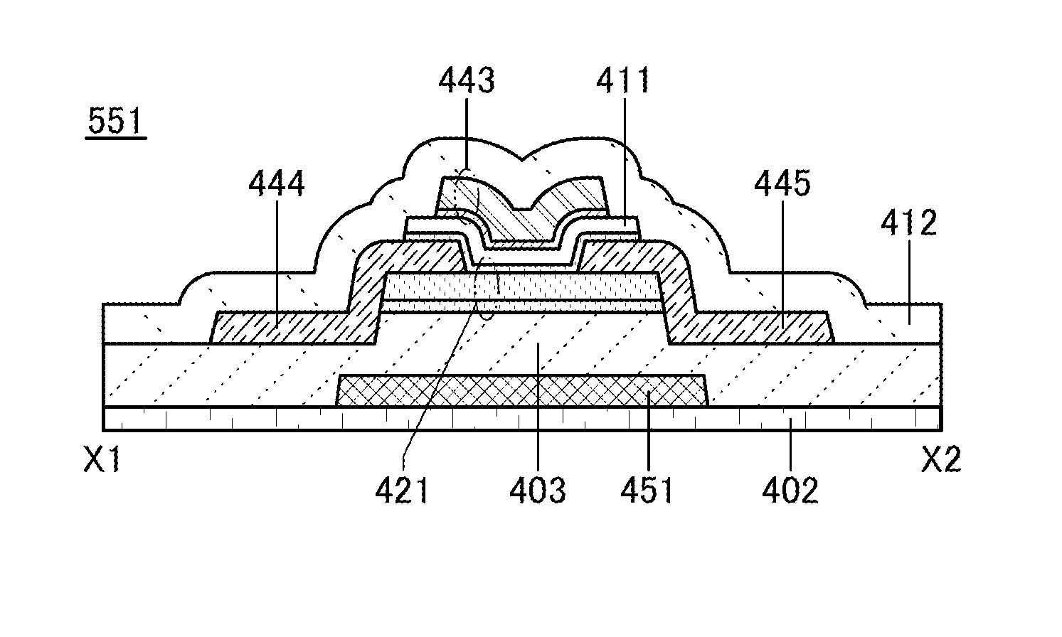
[0138]In this embodiment, structure examples of a pixel of one embodiment of the present invention are described.

[0139]FIG. 5 is a layout example of the pixel 21, which can be used in the above embodiment. Note that the wirings, conductive layers, and semiconductor layers using the same hatch pattern in FIG. 5 can be formed using the same material in the same process.

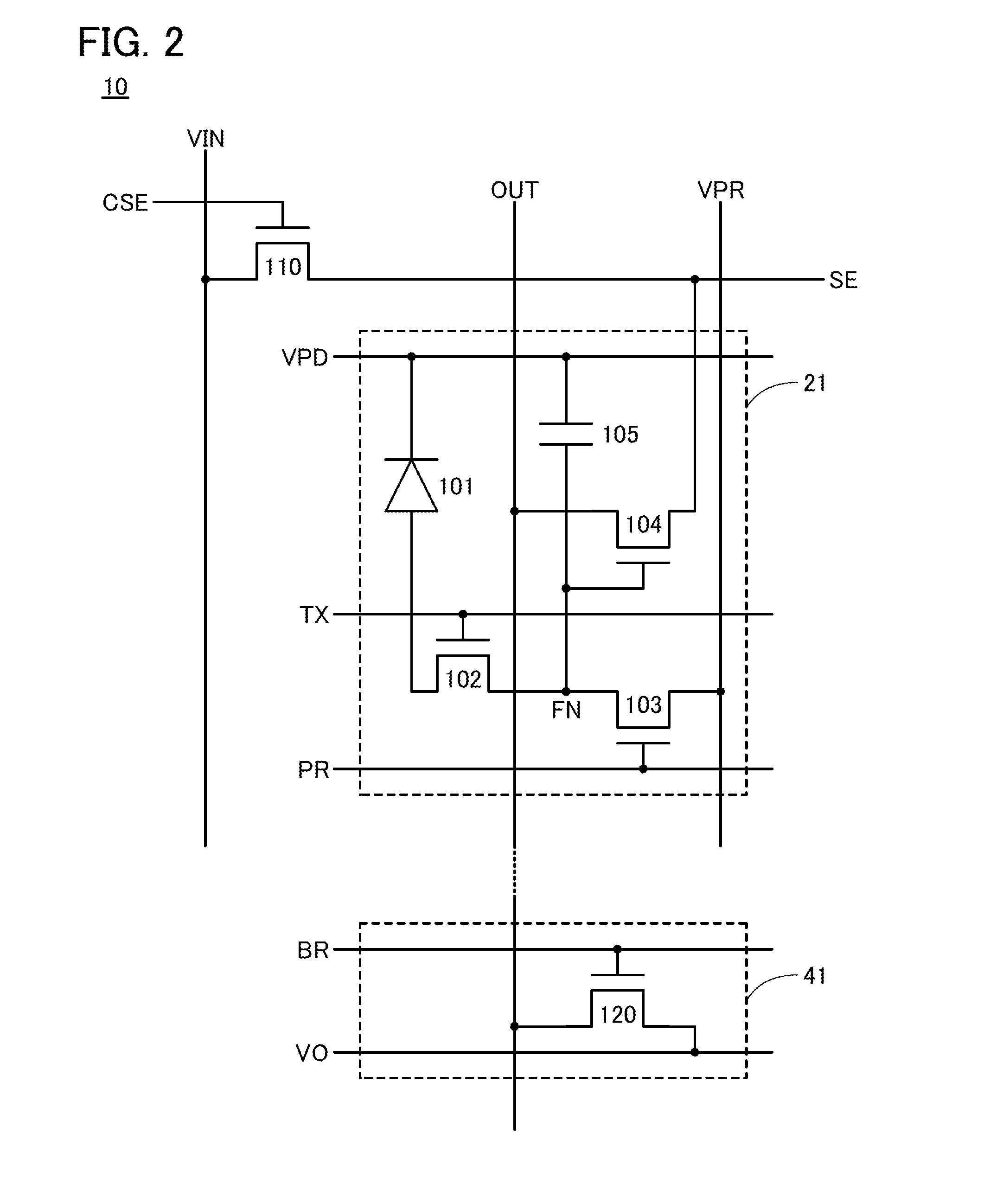
[0140]The pixel 21 in FIG. 5 includes the transistors 102, 103, and 104 and the capacitor 105. Detailed description of connection relationship between the elements is skipped because the description of FIG. 2 can be referred to. Although the photoelectric conversion element 101 is not shown in FIG. 5, the photoelectric conversion element 101 is connected to a conductive layer 250.

[0141]A semiconductor layer 221 serves as an active layer of the transistors 102 and 103. That is, the semiconductor layer 221 is shared by the transistors 102 and 103. A semiconductor layer 222 serves as an active layer of the transistor 104.

[...

embodiment 3

[0173]In this embodiment, an imaging device including the semiconductor device of one embodiment of the present invention is described.

[0174]FIG. 10 illustrates a structure example of an imaging device 300. The imaging device 300 includes a photodetector portion 310 and a data processing portion 320.

[0175]The photodetector portion 310 includes circuits 20, 30, 40, 50, and 60. The pixel portion and the circuit described in the above embodiments can be used for the pixel portion 20 and the circuits 30 and 40.

[0176]The circuit 50 has a function of converting an analog signal input from the circuit 40 into a digital signal. The circuit 50 can be composed of an A / D converter and the like.

[0177]The circuit 60 is a driving circuit having a function of reading a digital signal input from the circuit 50. The circuit 60 includes a selection circuit. The selection circuit can be formed using a transistor. The transistor can be an OS transistor or the like.

[0178]The data processing portion 320 ...


PUM


Abstract

Provided is a novel semiconductor device, a semiconductor device with reduced area, or a versatile semiconductor device. The semiconductor device includes a pixel portion including a first pixel, a second pixel, a third pixel, and a fourth pixel; a first switch and a second switch located outside the first to fourth pixels; a first wiring located outside the first to fourth pixels; a second wiring electrically connected to the first and second pixels; and a third wiring electrically connected to the third and fourth pixels. A first terminal of the first switch is electrically connected to the first wiring. A second terminal of the first switch is electrically connected to the second wiring. A first terminal of the second switch is electrically connected to the first wiring. A second terminal of the second switch is electrically connected to the third wiring.

Description

BACKGROUND OF THE INVENTION[0001]1. Field of the Invention[0002]One embodiment of the present invention relates to a semiconductor device, an imaging device, and an electronic device.[0003]One embodiment of the present invention is not limited to the above technical field. The technical field of one embodiment of the invention disclosed in this specification and the like relates to an object, a method, or a manufacturing method. One embodiment of the present invention relates to a process, a machine, manufacture, or a composition of matter. One embodiment of the present invention relates to a semiconductor device, a display device, a lighting device, a power storage device, a memory device, or a driving method or manufacturing method thereof.[0004]2. Description of the Related Art[0005]A technological development of a photodetector including a photodetector circuit (also referred to as an optical sensor) capable of generating data having a value corresponding to the illuminance of i...

Claims


Application Information

Patent Timeline
IPC IPC(8): H01L27/146H01L31/032H04N5/225H01L29/786
CPCH01L27/14643H01L27/14636H04N5/2253H01L29/7869H01L31/0322H01L27/14612H01L27/14609H01L27/14641H01L27/1225H04N25/709H04N25/76H04N25/778H01L27/14603H04N23/54
Inventor OHMARU, TAKURO
Owner SEMICON ENERGY LAB CO LTD
Why Eureka
Try Eureka