OLED device packaging method and OLED device packaged with same

a technology of oled devices and packaging methods, which is applied in the direction of organic semiconductor devices, solid-state devices, thermoelectric devices, etc., can solve the problems that the techniques of this area have not been popularized, and achieve the effects of extending the life of the oled device, excellent packaging effect, and simple process

Active Publication Date: 2016-06-09
TCL CHINA STAR OPTOELECTRONICS TECH CO LTD
View PDF4 Cites 3 Cited by
  • Summary
  • Abstract
  • Description
  • Claims
  • Application Information

AI Technical Summary

Benefits of technology

[0008]An object of the present invention is to provide an OLED device packaging method, which has a simple process, provides an excellent effect of packaging, effectively extends the life span of the OLED device, and requires a low cost.

Problems solved by technology

However, the UV resins are organic materials and exhibit relatively large gaps between molecules after being cured so that moisture and oxygen may easily penetrate the medium to reach the interior enclosed area.
However, to apply metal welding between two flat panels of glass, due to the limitations that the welding temperature is not allowed to be excessively high (the temperature of a welded zone being not allowed to exceed 900° C.) and the thermal expansion coefficients of commonly used metals are different from glass (which may lead to stress), techniques of this area have not been popularized.
It is thus an important issue to handle welding of glass substrate by developing a novel metal welding technique.

Method used


Image

  • OLED device packaging method and OLED device packaged with same
  • OLED device packaging method and OLED device packaged with same
  • OLED device packaging method and OLED device packaged with same

Examples


Embodiment Construction

[0047]To further expound the technical solution adopted in the present invention and the advantages thereof, a detailed description is given to a preferred embodiment of the present invention and the attached drawings.

[0048]Referring to FIGS. 1 and 2, an OLED device packaging method comprises the following steps:

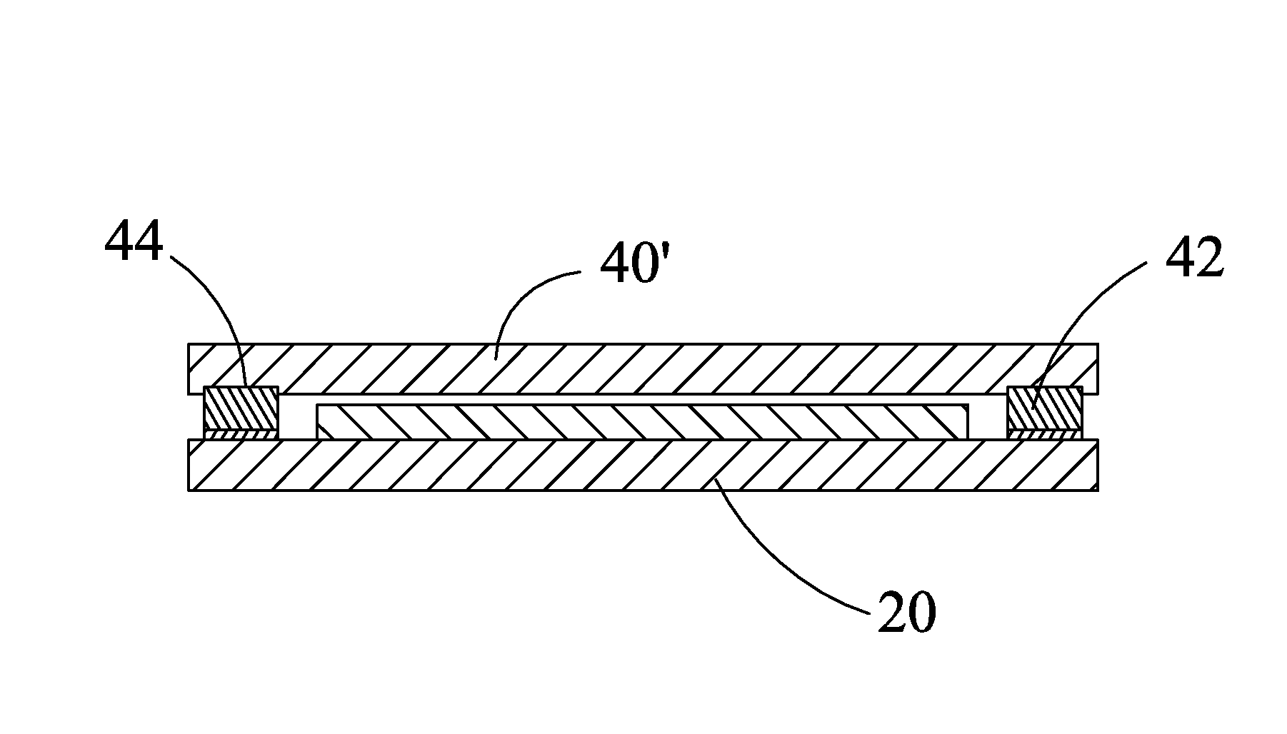
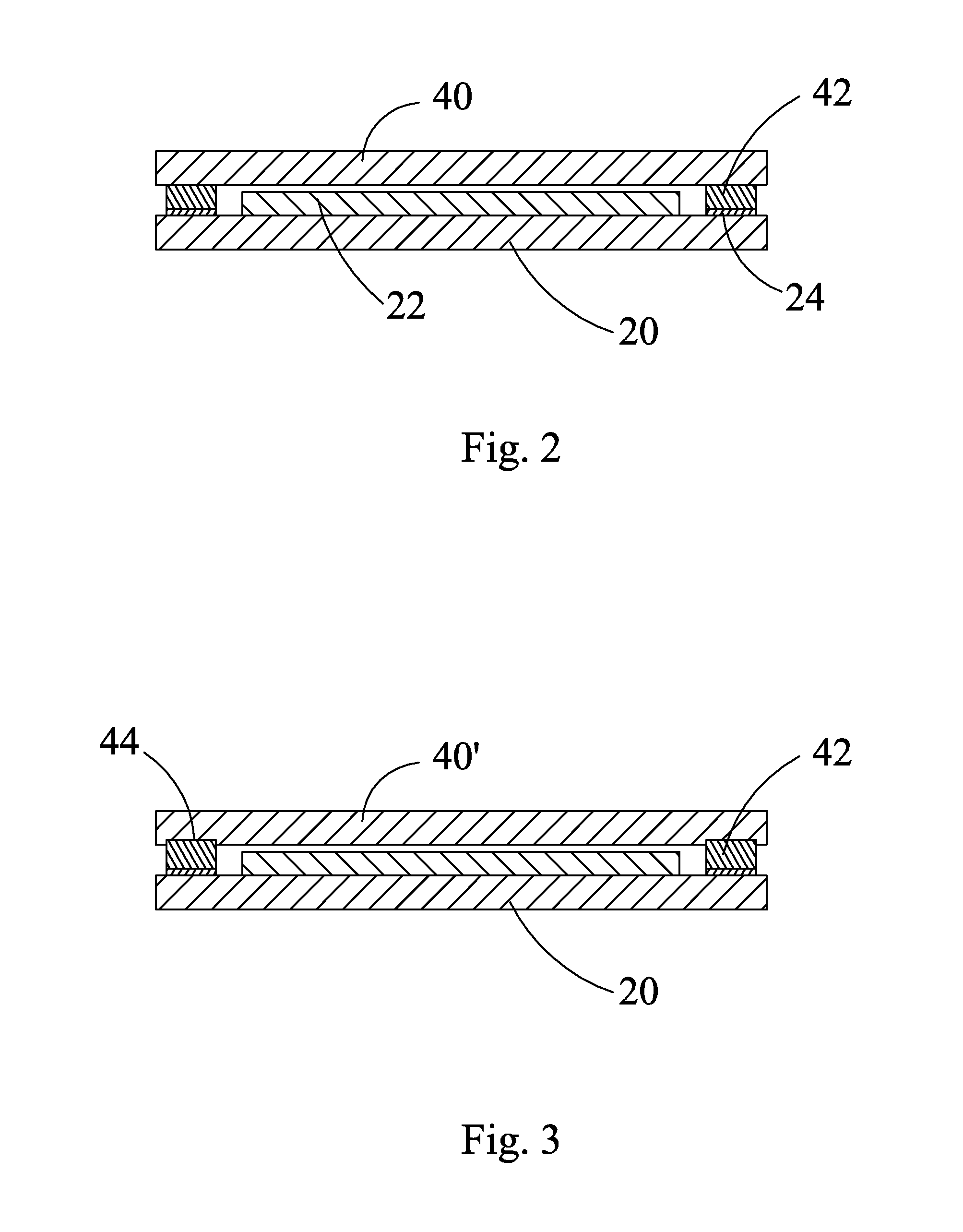
[0049]Step 1: providing an OLED substrate 20, wherein the OLED substrate 20 comprises an OLED unit 22 formed thereon.

[0050]The OLED substrate 20 is a transparent substrate, preferably a glass substrate. The OLED unit 22 generally comprises: an anode, an organic layer formed on the anode, and a cathode formed on the organic layer. It is noted that the organic layer generally comprises a hole transport layer (HTL) formed on the anode, an emitting material layer (EML) formed on the hole transport layer, and an electron transport layer (ETL) formed on the emitting material layer, each being formed by means of vapor deposition.

[0051]Step 2: using insulation material to form a fir...


PUM


Abstract

The present invention provides an OLED device packaging method and an OLED device packaged with the method. The method includes: (1) providing an OLED substrate (20), wherein the OLED substrate (20) includes an OLED unit (22) formed thereon; (2) using insulation material to form a first frame (24) on the OLED substrate (20), wherein the first frame (24) is arranged around and outside the OLED unit (22); (3) providing a packaging cover (40); (4) using a low-temperature metal conductive adhesive tape to form a second frame (42) on the packaging cover (40) to correspond in position to the first frame (24), wherein the second frame (42) has a frame member width that is smaller than a frame member width of the first frame (24); (5) aligning and laminating the packaging cover (40) that includes the second frame (42) formed thereon and the OLED substrate (20) that comprises the first frame (24) formed thereon in a vacuum environment; and (6) melting the second frame (42) to have the packaging cover (40) and the OLED substrate (20) bonded together.

Description

BACKGROUND OF THE INVENTION[0001]1. Field of the Invention[0002]The present invention relates to the field of OLED (Organic Light Emitting Display) device packaging techniques, and in particular to an OLED device packaging method and an OLED packaged with the method.[0003]2. The Related Arts[0004]In the field of displaying technology, flat panel display devices gradually take the place of CRT (Cathode Ray Tube) display devices. Conventional flat panel display devices generally include liquid crystal displays (LCDs) and organic light emitting displays (OLEDs). Planar lighting technology is a novel light source and the development thereof has already gotten close to the stage of commercialized mass production. In the flat panel display and planar lighting technologies, bonding and welding between two flat glass panels is a technique of vital importance and the result of packaging thereof will directly affect the performance of the devices.[0005]Ultraviolet (UV) curing is the technique...

Claims


Application Information

Patent Timeline
Patent Type & Authority Applications(United States)
IPC IPC(8): H01L51/52H01L51/56
CPCH01L51/5246H01L2251/558H01L51/56H10K50/841H10K50/8426H10K2102/351H10K71/00
Inventor LIU, YAWEI
Owner TCL CHINA STAR OPTOELECTRONICS TECH CO LTD
Why Eureka
Try Eureka