

Hybrid integration of edge-coupled chips
a technology of edge-coupled chips and hybrid optical sources, which is applied in the direction of optical elements, semiconductor lasers, instruments, etc., can solve the problems of material for light emission, difficult to achieve low-cost, efficient optical sources such as lasers, and difficult to implement silicon-photonic links. achieve the effect of reducing separation
- Summary
- Abstract
- Description
- Claims
- Application Information
AI Technical Summary
Benefits of technology
Problems solved by technology
Method used
Image

Examples
Embodiment Construction
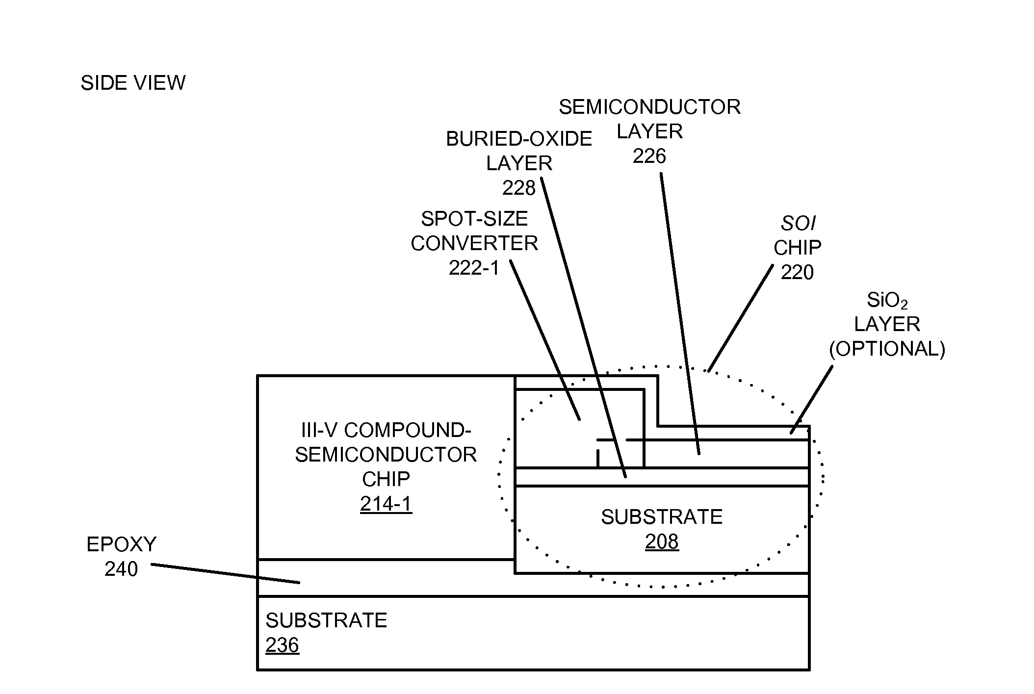
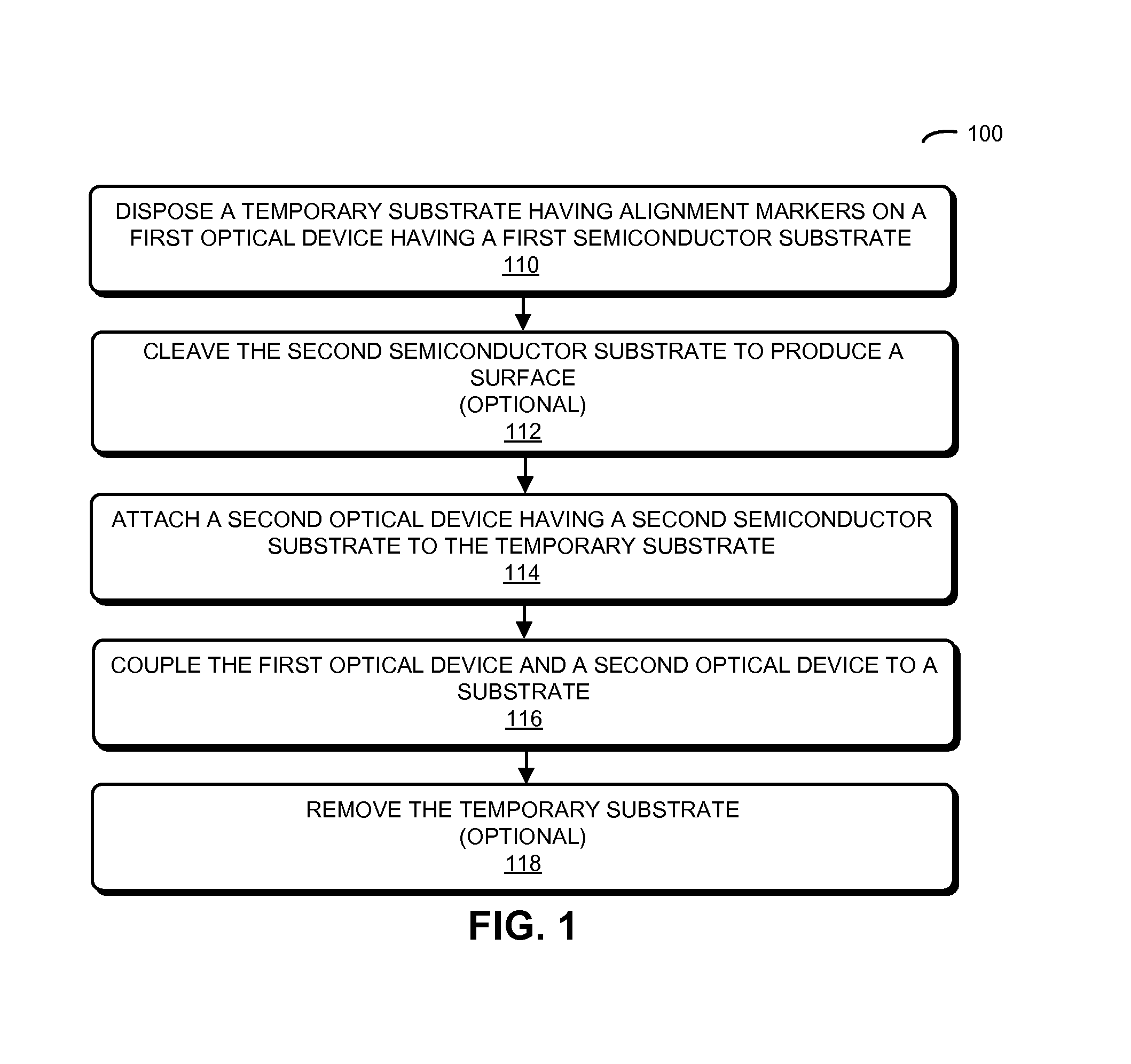
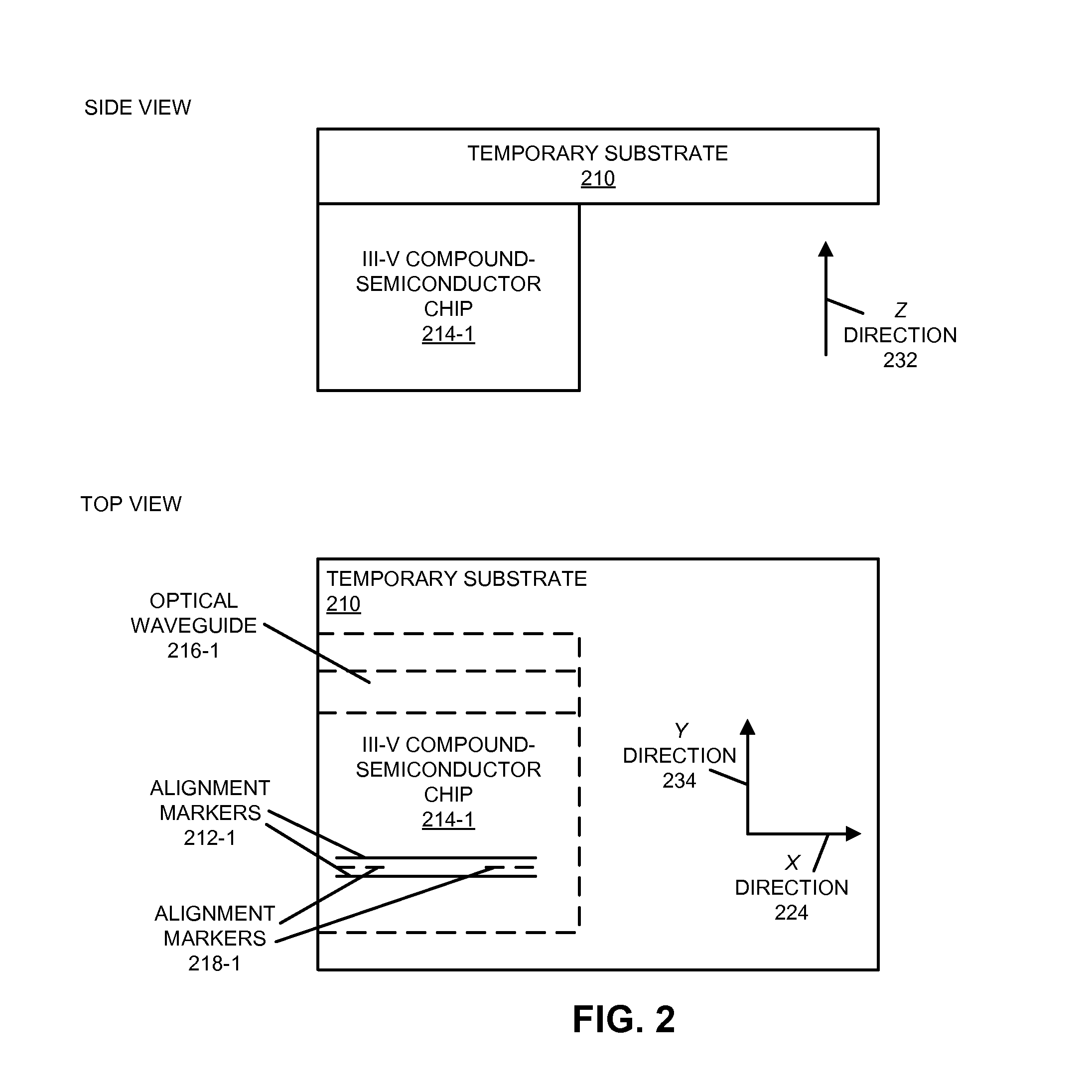
[0039]Embodiments of a co-planar hybrid optical source, a system that includes the hybrid optical source, and a method for fabricating the hybrid optical source are described. During this fabrication technique, a III-V compound-semiconductor active gain medium is integrated with a silicon-on-insulator (SOI) chip (or wafer) using edge coupling to form a co-planar hybrid optical source. Using a backside etching-assisted cleaving technique, and a temporary transparent substrate with alignment markers, a III-V compound-semiconductor chip with proper edge polish and coating can be integrated with a processed SOI chip (or wafer) with accurate alignment. This fabrication technique may significantly reduce the alignment complexity when fabricating the hybrid optical source, and may enable wafer-scale integration.
[0040]The fabrication technique may allow fabrication of a high-yield, low-cost and high-performance hybrid optical source. Consequently, the fabrication technique may enable the us...
PUM
 Abstract
Description
Claims
Application Information