Connection pads for a fingerprint sensing device

a fingerprint sensing and connection pad technology, applied in the field of sensing devices, can solve the problems of reducing affecting the assembly and design of the fingerprint sensor, and affecting the accuracy of the sensing device, so as to reduce the number of processing steps, and improve the effect of reliability

Active Publication Date: 2016-07-21
FINGERPRINT CARDS ANACATUM IP AB
View PDF10 Cites 17 Cited by
  • Summary
  • Abstract
  • Description
  • Claims
  • Application Information

AI Technical Summary

Benefits of technology

[0023]According to one embodiment of the invention, the connection plane may be arranged as an integral part of the topmost metal layer of the fingerprint sensing device. Thereby, the conductive portions of the connection plane and the conductive material of the connection pad may be formed in the in the same process step which reduces the number of processing steps required in the manufacturing process compared to if the connection plane and connection pads are made in different steps, and which also provides a more reliable electrical connection between the connection pad and the sensing circuitry.
[0024]Furthermore, the connection plane may advantageously be arranged in the sensing plane, meaning that the deposition of the connection plane coincides with the deposition of the sensing elements. Ther...

Problems solved by technology

Accordingly, protruding wire bonds introduce constraints in the assembly and design of a fingerprint sensor.
In addition, any protruding portions of an electrically conductive feature, relative to the pixels, such as e.g. a wire bond, will inevitably deteriorate the ...

Method used


Image

  • Connection pads for a fingerprint sensing device
  • Connection pads for a fingerprint sensing device
  • Connection pads for a fingerprint sensing device

Examples


Embodiment Construction

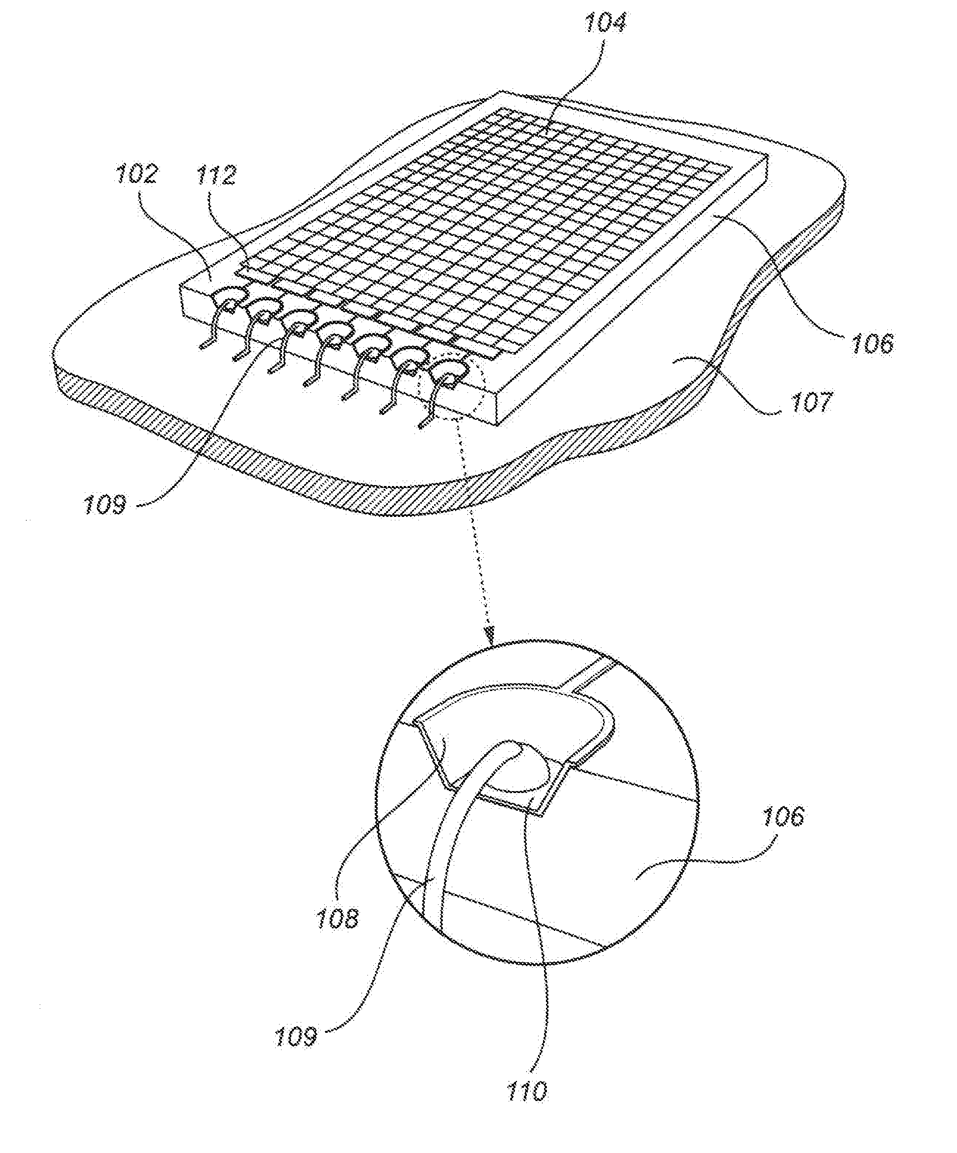
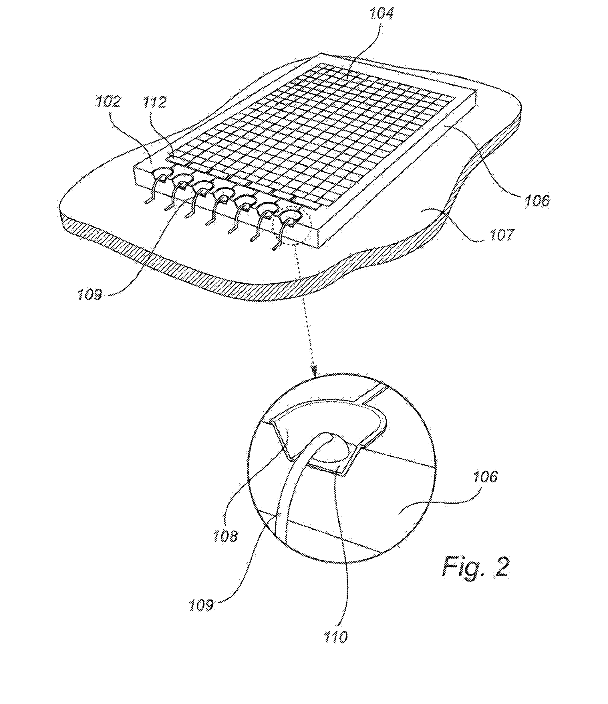
[0053]In the present detailed description, various embodiments of a fingerprint sensing device according to the present invention are mainly discussed with reference to a capacitive fingerprint sensing device. A method for manufacturing a connection pad for use in a fingerprint sensing device is also discussed. The manufacturing method may advantageously be used for the fabrication of connection pads also for other types of devices, such as for example an optical or RF-sensing device.

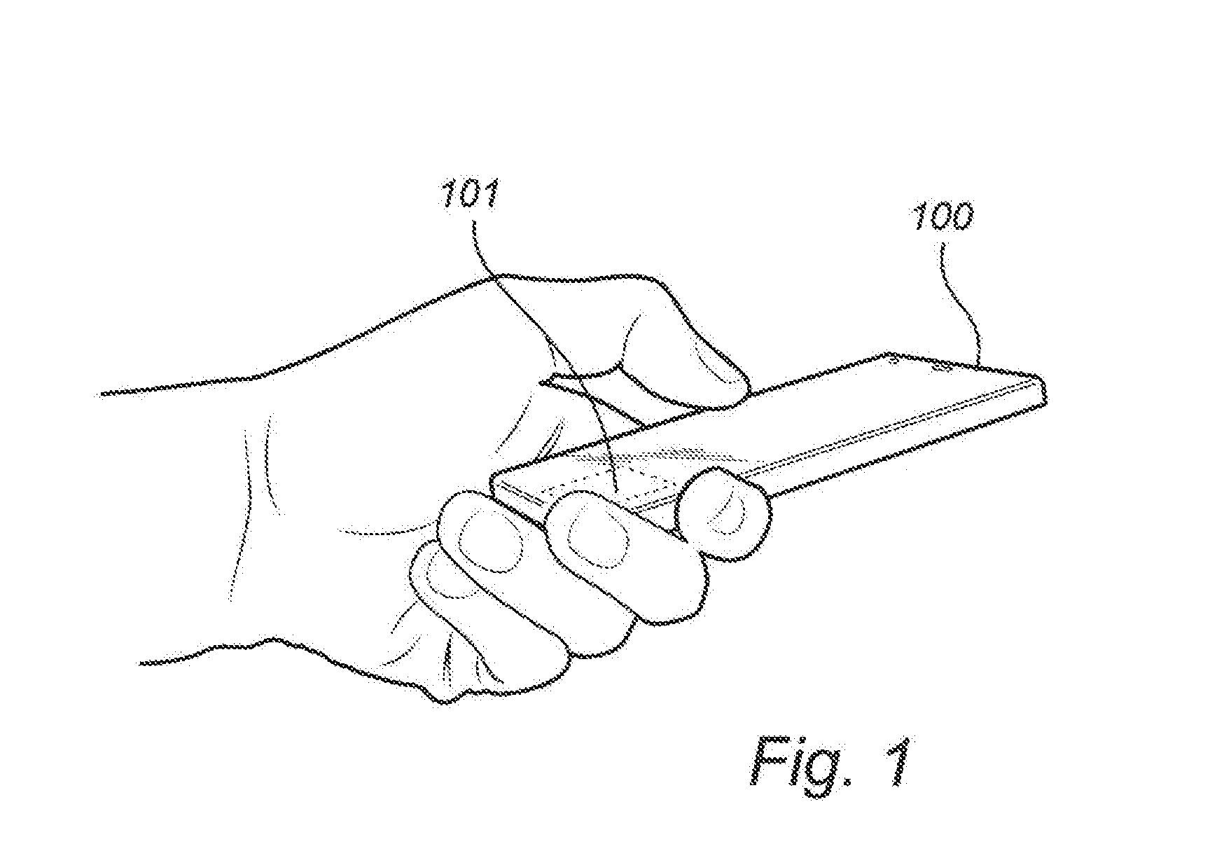
[0054]FIG. 1 is a schematic illustration of a handheld device 100 comprising a fingerprint sensing device 101. A fingerprint sensing device 101 can be used in for example a mobile phone, a tablet computer, a portable computer or any other electronic device as a way to identify and / or authenticate a user.

[0055]FIG. 2 is a schematic illustration of a fingerprint sensing device 102 exposing a plurality of sensing elements 104 arranged in an array of sensing elements 104. Each sensing element 104 comprises ...


PUM


Abstract

A fingerprint sensing device comprising sensing circuitry comprising a plurality of sensing elements, each sensing element comprising a sensing structure arranged in a sensing plane and facing a surface of the capacitive fingerprint sensing device, each of the sensing elements being configured to provide a signal indicative of an electromagnetic coupling between the sensing structure and a finger placed on the surface of the fingerprint sensing device; and a plurality of connection pads electrically connected to the sensing circuitry for providing an electrical connection between the sensing circuitry and readout circuitry, wherein each of the connection pads is separately recessed in relation to the sensing plane such that each connection pad has a floor in a floor plane, and wherein each connection pad is separated from an adjacent connection pad through a portion of the sensing device being elevated in relation to the floor plane.

Description

FIELD OF THE INVENTION[0001]The present invention relates to a sensing device. More particularly, the present invention relates to a device for sensing fingerprints.TECHNICAL BACKGROUND[0002]As the development of biometric devices for identity verification, and in particular of fingerprint sensing devices, has lead to devices which are made smaller, cheaper and more energy efficient, the possible applications for such devices are increasing.[0003]In particular fingerprint sensing has been adopted more and more in, for example, consumer electronic devices, due to small form factor, relatively beneficial cost / performance factor and high user acceptance (in particular in comparison to retina scanning etc).[0004]Capacitive fingerprint sensing devices, built based on CMOS technology for providing the fingerprint sensing elements and auxiliary logic circuitry, are increasingly popular as such sensing devices can be made both small and energy efficient while being able to identify a finger...

Claims


Application Information

Patent Timeline
IPC IPC(8): G06K9/00H01L23/00
CPCG06K9/0002H01L24/09H01L24/49H01L24/03H01L2224/035H01L2224/05022H01L2224/06179H01L2224/48148H01L2224/033H01L2224/04042H01L24/05H01L2224/48091H01L2224/48465H01L2224/48471H01L2224/85186H01L2924/00014H01L2924/10157H01L24/48H01L2224/0345H01L2224/03462H01L2224/05624H01L2224/05647H01L2224/49175H01L2924/181H01L2924/10155H01L2224/48463H01L2224/48453G06V40/1306H01L2224/45099H01L2924/00H01L2924/00012H01L2224/4554
Inventor JAGEMALM, PONTUSLUNDAHL, KARLSLOTTNER, MATSTHORNBLOM, HANSJULIAN, OJIE
Owner FINGERPRINT CARDS ANACATUM IP AB
Why Eureka
Try Eureka