Process substrate with crystal orientation mark, method of detecting crystal orientation, and reading device of crystal orientation mark

a technology of reading device and substrate, which is applied in the direction of semiconductor devices, semiconductor/solid-state device details, instruments, etc., can solve the problems of difficult to adjust production quantities, difficult to realize a sufficiently accurate alignment inexpensively, and difficult to adjust market penetration by small businesses, etc., to achieve high precision alignment, simple process, and simple process

Active Publication Date: 2016-07-21
NAT INST OF ADVANCED IND SCI & TECH
View PDF4 Cites 3 Cited by
  • Summary
  • Abstract
  • Description
  • Claims
  • Application Information

AI Technical Summary

Benefits of technology

[0021]A process substrate with crystal orientation mark of the present invention is configured such that a marking region for crystal orientation detection is formed at two locations in an outer edge portion of the process substrate, and an in-plane crystal axis of the process substrate is determined by using the marking regions for crystal orientation detection of those two locations. Therefore, according to the present invention, it is possible to add a crystal orientation mark, which enables high precision alignment, on a process substrate inexpensively by a simple process.
[0022]Moreover, the process substrate with crystal orientation mark of the present invention is configured such that a pattern for demonstrating predetermined information relating to the process substrate is formed in a straight line region connecting the marking regions for crystal orientation detection at the two locations, that is, a marking region for information. Therefore, according to the present invention, it is possible to add predetermined information relating to the process substrate on the process substrate inexpensively by a simple process.
[0023]Since in the process substrate with crystal orientation mark of the present invention, a marking region for crystal orientation detection and a marking region for information can be formed in a same process by configuring the marking to be at least one straight line or broken line, the process of forming the crystal orientation mark becomes simpler and more inexpensive.
[0024]According to a process substrate with crystal orientation mark of the present invention, a crystal orientation mark can be easily formed by laser marking by making up at least part of the marking with an array of plurality of dots.
[0025]According to a process substrate with crystal orientation mark of the present invention, it is possible to display a crystal plane orientation on a process substrate in an inexpensive and simple manner by configuring the pattern of the marking region for information to be a pattern that indicates information to determine the crystal plane orientation of the process substrate.
[0026]According to a process substrate with crystal orientation mark of the present invention, it is possible to form a crystal orientation mark which enables high precision alignment inexpensively by a simple process even when a wafer having a diameter of not more than 20 mm is adopted as the process substrate.

Problems solved by technology

However, although such a large scale manufacturing system will contribute to reduction of unit cost for manufacturing a chip in a production of small-kinds in large quantities, it hardly responds to the demand of a production of many-kinds in small quantities, and makes it difficult to adjust the production quantities in response to market conditions, also making the market penetration by small businesses difficult.
As a result of that, it has been revealed that in the case of a small-diameter wafer, it is necessary to form an orientation flat or a notch in a very small size, and therefore, it is difficult to realize a sufficiently accurate alignment inexpensively.
Moreover, it is also revealed that forming a small notch in a small-diameter wafer will take a lot of time and effort for surface finishing, and is against the demand for cost reduction in this respect as well.
Furthermore, a method of performing laser drawing to discriminate the kind of wafer and the like is also against the purpose of developing a small-diameter wafer as described above, since it is necessary to perform a laser drawing process in addition to the process of forming an orientation flat or a notch, thus causing increases in the cost and the number of processes.

Method used


Image

  • Process substrate with crystal orientation mark, method of detecting crystal orientation, and reading device of crystal orientation mark
  • Process substrate with crystal orientation mark, method of detecting crystal orientation, and reading device of crystal orientation mark
  • Process substrate with crystal orientation mark, method of detecting crystal orientation, and reading device of crystal orientation mark

Examples


embodiment 1

of the Present Invention

[0034]Hereafter, Embodiment 1 of the present invention will be describe by using FIGS. 1 to 5 by taking as an example a case in which the present invention is applied to a semiconductor wafer.

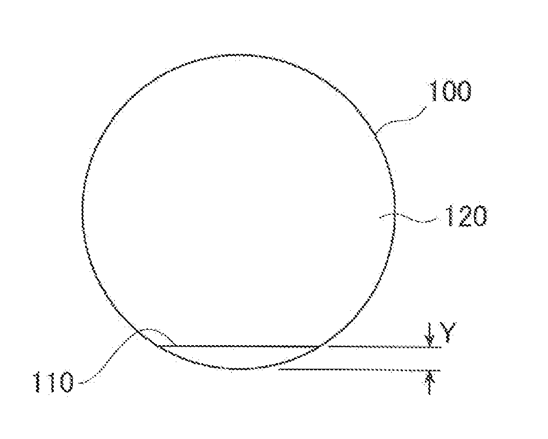
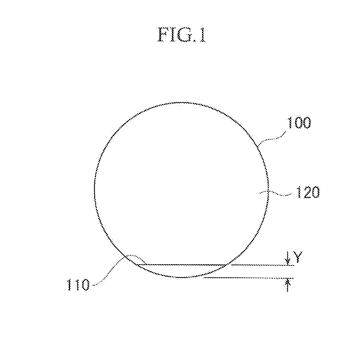
[0035]FIG. 1 is a plan view to conceptually show a wafer with a crystal orientation mark (hereafter, simply referred to as “wafer”) 100 according to Embodiment 1. As shown in FIG. 1, the wafer 100 according to Embodiment 1 is formed with a crystal orientation mark 110.

[0036]The dimension of the wafer 100 is not particularly limited. However, this embodiment is particularly beneficial when it is applied to a small-diameter wafer having a diameter of not more than 20 mm (for example, a diameter of 0.5 inches).

[0037]The crystal orientation mark 110 is formed along a predetermined in-plane crystal orientation of the wafer 100. When the diameter of the wafer 100 is 0.5 inches, it is preferable that a distance Y between an outer edge of the wafer 100 and the crystal orientatio...


PUM


Abstract

To provide a crystal orientation mark which can be formed easily and inexpensively, and which enables to perform high precision alignment and allows information other than crystal orientation to be included, even for a small diameter process substrate. A crystal orientation mark is drawn on the surface of the process substrate. The crystal orientation mark includes a marking region for crystal orientation detection, and a marking region for information. The marking region for crystal orientation detection is provided at two locations in an outer edge portion of the process substrate to be used for the alignment of the process substrate. The marking region for information is provided on a straight-line region connecting the marking regions for crystal orientation detection at the two locations, and includes a pattern for demonstrating predetermined information relating to the process substrate.

Description

CROSS-REFERENCE TO RELATED APPLICATIONS[0001]This application is a U.S. National Stage Application, which claims the benefit under 35 U.S.C. §371 of PCT International Patent Application No. PCT / JP2014 / 069570, filed Jul. 24, 2014, which claims the foreign priority benefit under 35 U.S.C. §119 of Japanese Patent Application No. 2013-170122, filed Aug. 20, 2013, the contents of which are incorporated herein by reference.TECHNICAL FIELD[0002]The present invention relates to a process substrate, i.e. a substrate to be processed, added with a crystal orientation mark, and a method and apparatus for detecting crystal orientation by using such process substrate. The present invention is suitable for application to a small-diameter semiconductor wafer having, for example, a diameter of not more than 20 mm.BACKGROUND ART[0003]Conventional process substrates with crystal orientation mark will be described by taking a semiconductor wafer as an example.[0004]Conventionally, a semiconductor wafer...

Claims


Application Information

Patent Timeline
Patent Type & Authority Applications(United States)
IPC IPC(8): H01L23/544H01L21/67G01B11/14H01L29/04
CPCH01L23/544H01L29/045H01L21/67259H01L2223/54493H01L2223/54426H01L2223/5442G01B11/14H01L21/67282H01L21/67294H01L2223/54453H01L2924/0002H01L2924/00
Inventor HARA, SHIROKHUMPUANG, SOMMAWANIKEDA, SHINICHI
Owner NAT INST OF ADVANCED IND SCI & TECH
Why Eureka
Try Eureka