Semiconductor device

a technology of semiconductor devices and semiconductors, applied in the direction of semiconductor devices, electrical equipment, transistors, etc., can solve the problems of deterioration of dielectric breakdown voltage, drop in processing accuracy, and reliability decline, so as to reduce the gate-collector capacitance, reduce the uneven surface of the device, and increase the switching speed

Active Publication Date: 2016-07-21
FUJI ELECTRIC CO LTD
View PDF16 Cites 10 Cited by
  • Summary
  • Abstract
  • Description
  • Claims
  • Application Information

AI Technical Summary

Benefits of technology

[0028]Using the aforementioned aspect of the present invention, it is possible to reduce the gate-collector capacitance associated with the shield electrodes and to increase the switching speed.
[0029]The present invention, in at least one aspect, is capable of making the shield electrodes in the trench gate IGBT into thin films and, as a result, reducing the unevenness of the device surface, because the shield electrodes are composed of a material that has an electrical resistivity lower than those of the gate electrodes. Furthermore, in at least one aspect, the present invention is capable of increasing the processing accuracy for photolithography, favorably covering the unevenness of the interlayer insulating films and the metallic wiring, and improving the dielectric breakdown voltage and the electromigration resistance. By providing the shield electrodes, it is also possible to suppress the displacement current flowing into the gate electrodes during turn-ON and to control the rate of change in the collector current during turn-ON with excellent accuracy.

Problems solved by technology

However, when the shield electrodes are disposed above the floating p regions 13 in the trench gate IGBT, the shield electrodes cause the surface of the substrate to become uneven, thus creating a decline in reliability due to a drop in the processing accuracy for photolithography, a deterioration of the dielectric breakdown voltage due to a failure to cover an uneven interlayer insulating film and metallic wiring, electromigration-induced disconnection, and the like.

Method used


Image

  • Semiconductor device
  • Semiconductor device
  • Semiconductor device

Examples


embodiment 1

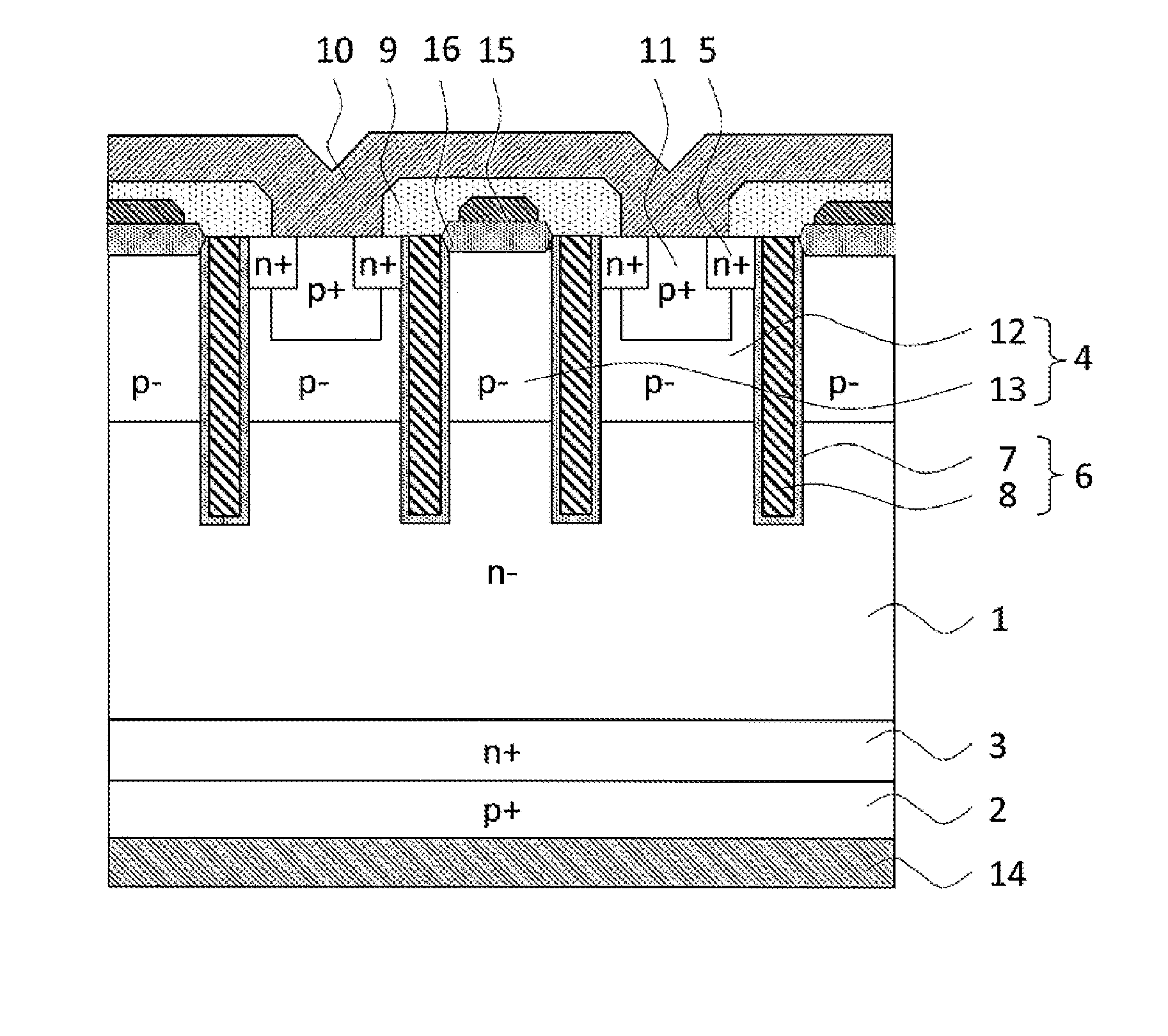
[0036]An n channel IGBT is described in detail below as one example of a semiconductor device according to Embodiment 1. This n channel IGBT has striped trench gates disposed therein extending in a longitudinal direction orthogonal to the lateral direction that the trenches are arranged.

[0037]FIG. 1 is a cross-sectional schematic view cut in the direction (the lateral direction) that the trench gates of the semiconductor device according to Embodiment 1 of the present invention are arranged. The semiconductor device according to Embodiment 1 is provided with an active region, which is shown in FIG. 1, in which current flows when the semiconductor device is in the ON state and a termination structure, which is not shown in the figures, for maintaining the breakdown voltage by reducing the electric field at the front surface-side of the semiconductor device.

[0038]In the active region, a p− layer 4 is provided on one surface layer of a silicon substrate that is provided with an n− drif...

embodiment 2

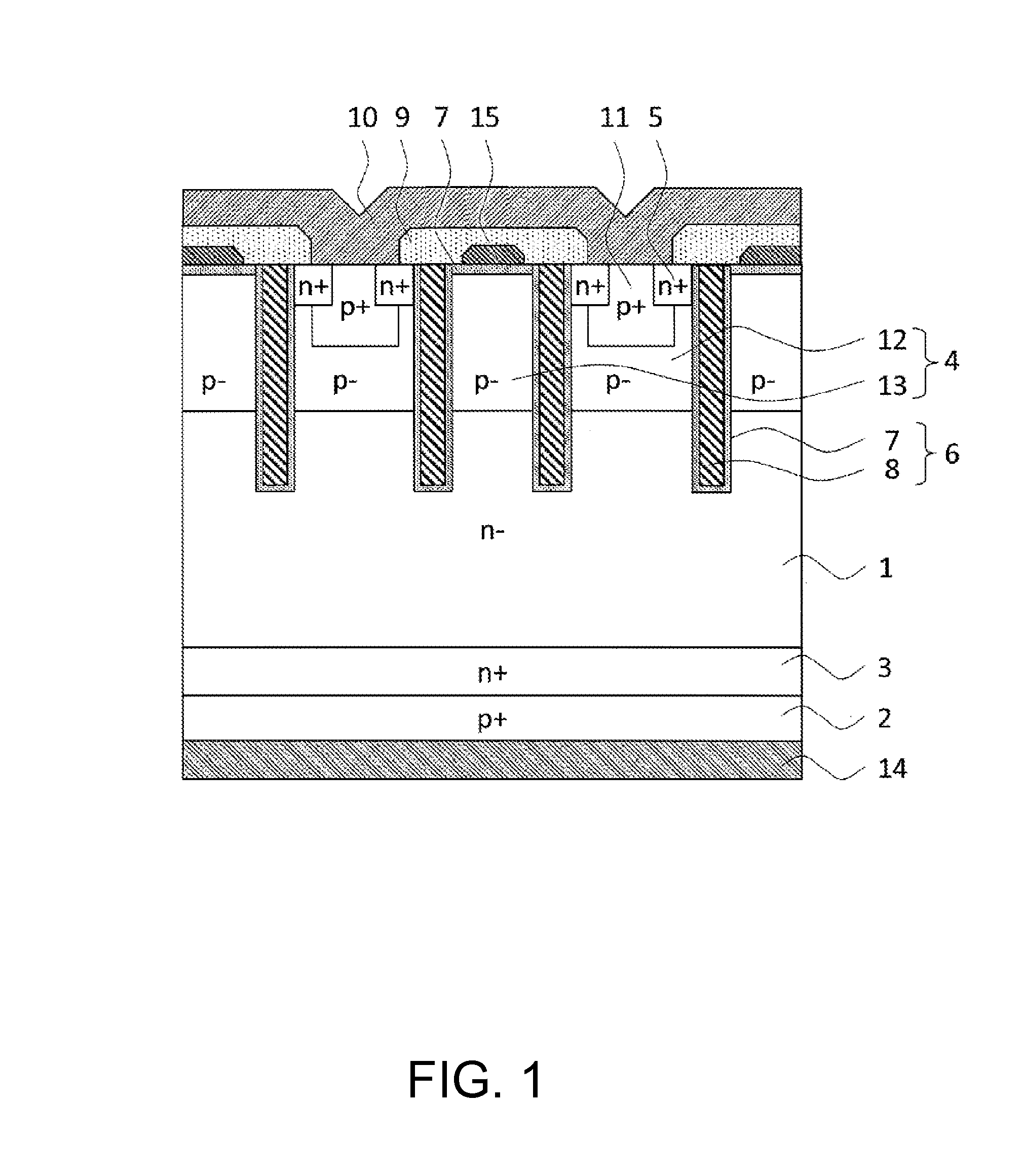
[0048]An n channel IGBT is described in detail below as one example of a semiconductor device according to Embodiment 2. This n channel IGBT has striped trench gates disposed therein extending in a longitudinal direction orthogonal to the lateral direction that the trenches are arranged.

[0049]FIG. 2 is a cross-sectional schematic view cut in the lateral direction that the trench gates of the semiconductor device according to Embodiment 2 of the present invention are arranged. FIG. 2 is different from FIG. 1 in that the shield electrodes 15 are electrically connected to the gate electrodes 8 on the upper portion of the trenches 6 and maintain the same electric potentials as those of the gate electrodes 8. With this configuration, it is possible to further improve the controllability of the rate of change in the collector current during turn-ON, because the connection distance between the shield electrodes 15 and the gate electrodes 8 is shortened and there is almost no voltage drop d...

embodiment 3

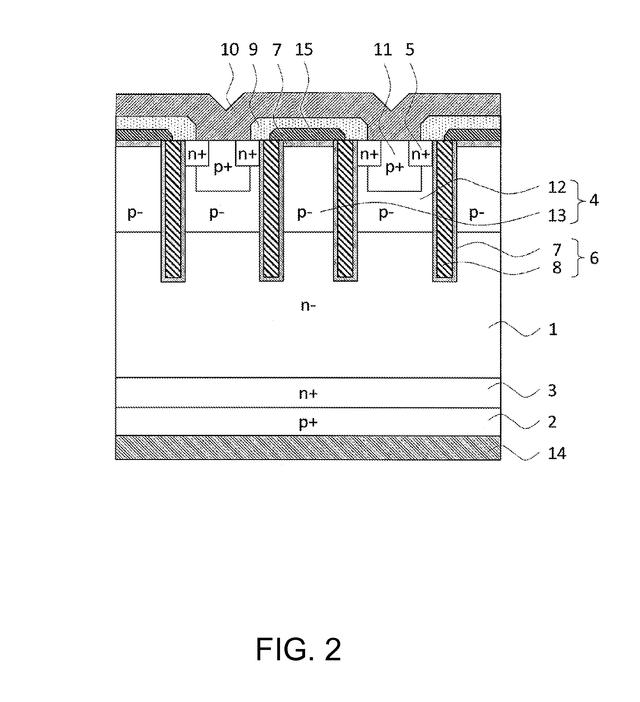
[0050]An n channel IGBT is described in detail below as one example of a semiconductor device according to Embodiment 3. This n channel IGBT has striped trench gates disposed thereon extending in a longitudinal direction orthogonal to the lateral direction that the trenches are arranged.

[0051]FIG. 3 is a cross-sectional schematic view cut in the lateral direction that the trench gates of the semiconductor device according to Embodiment 3 of the present invention are arranged. FIG. 3 is different from FIG. 1 in that the shield electrodes 15 are electrically insulated from the floating p regions 13 by thick insulating films 16 that are thicker than the gate insulating films 7. With this configuration, it is possible to reduce the gate-collector capacitance associated with the shield electrodes and to increase the switching speed because the film thickness of the thick insulating films 16 is large.

[0052]It is preferable that the thickness of the thick insulating films 16 be 100-800 nm,...


PUM


Abstract

A shield electrode is formed above a floating p region in a semiconductor layer and connected to a gate electrode in a trench. The shield electrode is composed of a material having an electrical resistivity lower than that of the gate electrode.

Description

BACKGROUND OF THE INVENTION[0001]1. Technical Field[0002]The present invention relates to a semiconductor device having a trench gate IGBT structure.[0003]2. Background Art[0004]As power converters continue to consume less power, there are increasing expectations for power devices, which play a central role in the power converters, to also consume less power. Among these power devices, voltage-driven insulated gate bipolar transistors (IGBTs) are being used. These IGBTs are capable of realizing low ON-voltages due to conductivity modulation and of easily controlling current by applying voltage to an insulated gate. Planar gate IGBTs, trench gate IGBTs, and the like are known as types of IGBTs, for example.[0005]The planar gate IGBTs have a metal oxide semiconductor (MOS) gate structure in which an oxide film and a gate electrode are provided on a flat part of the front surface-side of a silicon substrate. The trench gate IGBTs have a MOS gate structure in which an oxide film and gat...

Claims


Application Information

Patent Timeline
Patent Type & Authority Applications(United States)
IPC IPC(8): H01L29/739H01L27/082H01L29/08H01L29/06H01L29/10
CPCH01L29/7397H01L29/0696H01L27/0823H01L29/0804H01L29/0821H01L29/1095H01L29/0619H01L29/402
Inventor IKURA, YOSHIHIRO
Owner FUJI ELECTRIC CO LTD
Why Eureka
Try Eureka