A lateral trench insulated gate bipolar transistor and its preparation method

A technology of bipolar transistors and lateral trenches, applied in semiconductor/solid-state device manufacturing, semiconductor devices, electrical components, etc., can solve the problems of large turn-off loss, limited application, low electron mobility, etc., to reduce the forward guide The effect of reducing the voltage drop, improving the current drive capability, and increasing the layout area

Active Publication Date: 2017-03-22
SOUTHEAST UNIV
View PDF4 Cites 0 Cited by
  • Summary
  • Abstract
  • Description
  • Claims
  • Application Information

AI Technical Summary

Problems solved by technology

Although the traditional lateral SOI-LIGBT has advantages such as easy integration, it is a surface structure, and the mobility of electrons on the surface of the structure is low, so the current density is low. current drive capability, which greatly limits its application in high-power integrated circuits
[0004] The emergence of lateral trench insulated gate bipolar transistor (ordinary trench gate LIGBT) has greatly improved the current capability of LIGBT, but because it stores more carriers, and the holes are It needs to bypass the trench, so its turn-off speed is slow and the turn-off loss is large, and its application in high-power integrated circuits is also limited

Method used


Image

  • A lateral trench insulated gate bipolar transistor and its preparation method
  • A lateral trench insulated gate bipolar transistor and its preparation method
  • A lateral trench insulated gate bipolar transistor and its preparation method

Examples


Embodiment Construction

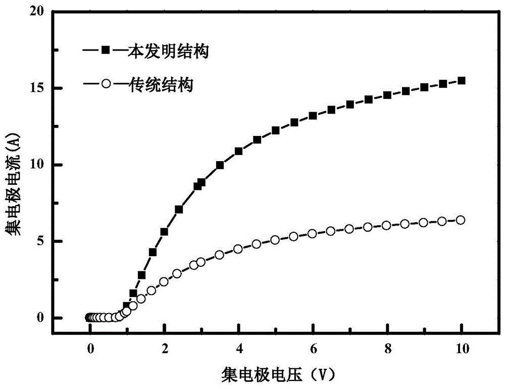
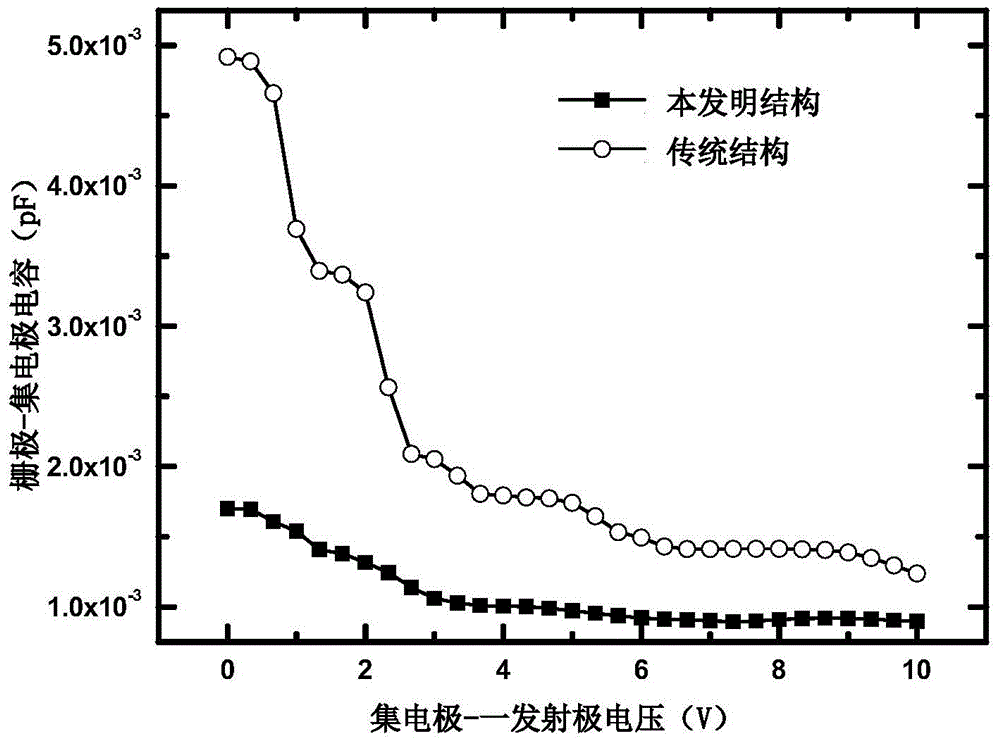
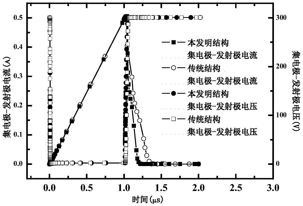
[0021] Combine below figure 2 , the present invention is described in detail, a lateral trench insulated gate bipolar transistor, comprising: a P-type substrate 1, a buried oxide layer 2 is arranged on the P-type substrate 1, and a N type drift region 3, an oxide layer 9 is provided above the upper surface of the N-type drift region 3, and a polysilicon gate 4, a P-type body region 8 and an N-type buffer layer 12 are provided below the upper surface of the N-type drift region 3, and An emitter region is provided in the P-type body region 8, an emitter aluminum electrode 7 is arranged on the emitter region, a P-type collector region 11 is arranged in the N-type buffer layer 12, and a P-type collector region 11 is arranged on the P-type collector region 11. There is a collector aluminum electrode 10, and the N-type buffer layer 12 and the P-type collector region 11 are located at one side of the N-type drift region 3, and the P-type body region 8 and the emitter region are loca...


PUM


Abstract

The invention discloses a transverse groove insulating gate bipolar transistor and a manufacturing method thereof. The transverse groove insulating gate bipolar transistor structurally comprises a P type substrate, a buried oxide layer, a drift region and a deep P type body region. A deep groove grid is arranged on one side of the drift region. A deep P type emitter region and a deep N type emitter region which are connected and extend into the drift region till a BOX layer are arranged in the deep P type body region. Emitter metal is arranged on the deep P type emitter region and the deep N type emitter region which are connected. An N type buffer layer and a P type collector region are arranged on the other side of the deep P type emitter region and the other side of the deep N type emitter region. Collector metal is arranged on the P type collector region. The semiconductor manufacturing method includes the steps of manufacturing the substrate, the buried oxide layer and an N type extension layer, forming an N type emitter, the P type body region and a P type emitter through the combination of the deep groove technology and the multi-extension and high-concentration ion multi-injection technology, forming the N type buffer layer and the P type collector region through the high-concentration ion injection technology, manufacturing a polycrystalline silicon grid through the groove grid technology, and forming electrodes through drilling and aluminum depositing.

Description

technical field [0001] The present invention mainly relates to the technical field of power semiconductor structures, specifically, it is especially suitable for high-power integrated circuits such as frequency conversion speed regulation, high-voltage power transmission, electric traction, frequency conversion household appliances, half-bridge drive circuits, and automobile production. Background technique [0002] The insulated gate bipolar transistor is a composite power structure evolved from the combination of the MOS gate structure and the bipolar transistor structure. It perfectly combines the advantages of fast switching speed of the MOS transistor and strong current capability of the bipolar transistor, and has been widely used It is used in frequency conversion home appliances, induction heating, industrial frequency conversion, photovoltaic power generation, wind power generation, locomotive traction and other fields. Among them, the silicon-on-insulator lateral i...

Claims


Application Information

Patent Timeline
Patent Type & Authority Patents(China)
IPC IPC(8): H01L29/739H01L29/41H01L21/28H01L21/331
CPCH01L29/41H01L29/66325H01L29/7393
Inventor 孙伟锋喻慧张龙祝靖陆生礼时龙兴
Owner SOUTHEAST UNIV
Why Eureka
Try Eureka