Processor model using a single large linear registers, with new interfacing signals supporting fifo-base I/O ports, and interrupt-driven burst transfers eliminating dma, bridges, and external I/O bus

Inactive Publication Date: 2016-08-04
UNIVERSITI TEKNOLOGI MALAYSIA +1
View PDF0 Cites 4 Cited by
  • Summary
  • Abstract
  • Description
  • Claims
  • Application Information

AI Technical Summary

Benefits of technology

[0017]A combination of these proven technologies supported by the corresponding CPU instruction set which enables these capabilities will result in a simple and powerful CPU architecture.
[0018]This invention describes a CPU model which uses a set of interfacing signals that support an interrupt-driven processing of FIFO-based I/O with synchronous burst data transfer. The CPU model su

Problems solved by technology

For example, troubleshooting a system with two arbiters and two bridges

Method used


Image

  • Processor model using a single large linear registers, with new interfacing signals supporting fifo-base I/O ports, and interrupt-driven burst transfers eliminating dma, bridges, and external I/O bus
  • Processor model using a single large linear registers, with new interfacing signals supporting fifo-base I/O ports, and interrupt-driven burst transfers eliminating dma, bridges, and external I/O bus
  • Processor model using a single large linear registers, with new interfacing signals supporting fifo-base I/O ports, and interrupt-driven burst transfers eliminating dma, bridges, and external I/O bus

Examples


first embodiment

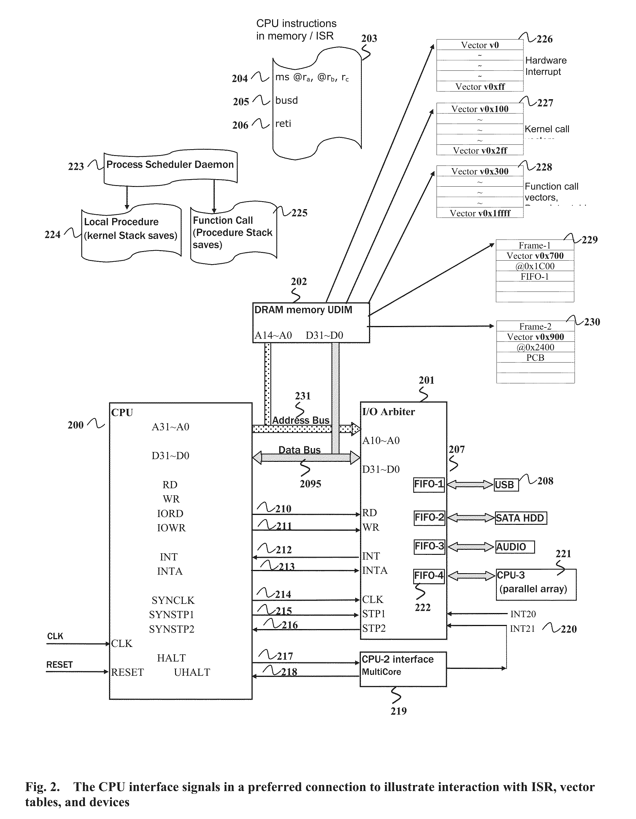
[0036]In the present invention, in a typical computing process involving data transfer to an I / O device which is through its FIFO, which in this example using FIFO-1 (207); the CPU (200) in kernel mode performs a certain data operation on a block of data in memory (202). The block of data is moved into all of the CPU registers (103) for maximum efficiency, a block of the register set at a time. After completion of operation, part of the block of registers is sent to some other memory locations.

[0037]Therefore a block of data needs to be read into a memory frame. Frame-1 (229) before a set of CPU operations can begin as described earlier. This is done by an I / O port to memory read in a synchronous burst data transfer. A CPU instruction (203) reads FIFO-1 (207) using the IORD signal (210), SYNCLK (214), SYNSTP1 (215), SYNSTP2 (216) signals until FIFO-1 (207) is empty. I / O arbiter (201) then activates SYNSTP2 (216) indicating end of data, in which CPU (200) stops reading.

[0038]Similarl...

second embodiment

[0040]In the present invention, which mimics a DMA transfer, another device or another CPU; CPU-2 (219), in a multiprocessor connection wants access to the data bus, it activates the INT signal (212) by way of I / O arbiter INT21 (an example number) signal (220), in which the CPU (200) jumps to the address assigned to the vector ID of CPU-2 (219). In the ISR (203), CPU instruction busd (205) disables all buses and executes a halt instruction in which CPU (200) activates the HALT signal (217) and stops executing instructions and wait for the hardware UHALT signal (218) from CPU-2 (219). At this point CPU-2 (219) gains access to CPU address (231) and data (209) buses until it activates UHALT signal (218) in which CPU (200) returns to normal and executes next instruction typically the reti (206) in which ISR exits interrupt.

[0041]In yet another alternative of a DMA transfer, CPU-3 (221) connected via L / O arbiter (201) using FIFO-4 (222) can access a block of memory, or a memory buffer, F...

third embodiment

[0042]In the present invention, a hardware interrupt mechanism is devised to create an almost zero housekeeping instructions for a fast and efficient interrupt processing in an ISR (203). An interrupt request is activated by means of the INT signal (212) from an external source such as an I / O arbiter (201). The CPU (200) answers with an INTA signal (213) after which, the interrupting device such as a USB device (208) by way of the L / O arbiter (201) places the vector ID of the device (208) on the data bus (209). CPU (200) then reads the vector ID and makes a direct jump to the vector ID address. Vector ‘va’ denotes the vector ‘a’ which is equivalent to the ID number and can take up to 18 bits in value. The CPU (200) recognizes only 256 hardware interrupt sources as reserved in the hardware interrupt vectors memory space (226).

[0043]Before executing the first instruction in the ISR (203) corresponding to the vector ID, current main control registers consisting of the FS (105), the FSP...


PUM


Abstract

A processor or CPU architecture that implements many enabling technologies proven to enhance data through put supporting the synchronous burst data transfer. The Input-Output (I/O) is uniformly viewed and treated as an individual First-In-First-Out (FIFO) device. Pluralities of memory areas are implemented for user stack, kernel stack, interrupt stack and procedure call stack. Only one I/O arbiter is necessary for a CPU model that arbitrates between a plurality of FIFOs substituting data caches for on-chip implementation, thus eliminating traditional data transfer techniques using Direct-Memory-Access (DMA), bus control and lock signals leaving just the interrupt signals and the new synchronous signals for an easy and streamlined system design and CPU model. Supporting an interrupt-driven, FIFO-based I/O and synchronous burst data transfer the CPU employs a simple linear large register sets without bank switching.

Description

TECHNICAL FIELD[0001]This invention relates to microprocessor and computer architecture.BACKGROUND OF THE INVENTIONHistory of CPU Architecture[0002]Many current processor or CPU architectures borrow from the IBM 360 (announced in 1964) which had both characteristics of CISC and RISC designs. The design already considered multiprocessing requirements with specific instructions as it was envisioned for the business and scientific computing needs. Most CPU designs were conceived for expected use around the Operating System (OS) software of the day, which were mostly proprietary. Up to this point, the computer was manufactured from discrete logic gates, resulting in the whole system occupying a few equivalent rooms in a house. The invention of a processor using discrete logic was already described in the U.S. Pat. No. 3,401,376 filed by G. H. Barnes et al in 1965, and granted patent in Sep. 10, 1968. Also U.S. Pat. No. 3,518,632 filed by R. Threadgold et al in 1967, which was granted pa...

Claims


Application Information

Patent Timeline
IPC IPC(8): G06F13/32G06F13/42G06F13/40
CPCG06F13/32G06F13/4282G06F13/4022
Inventor IBRAHIM, MUHAMMAD NASIR BINAZHARI, NAMAZI BINBAHARUM, ADAM BIN
Owner UNIVERSITI TEKNOLOGI MALAYSIA
Why Eureka
Try Eureka