Silicon carbide semiconductor device
- Summary
- Abstract
- Description
- Claims
- Application Information
AI Technical Summary
Benefits of technology
Problems solved by technology
Method used
Image
Examples
first embodiment
[0042]
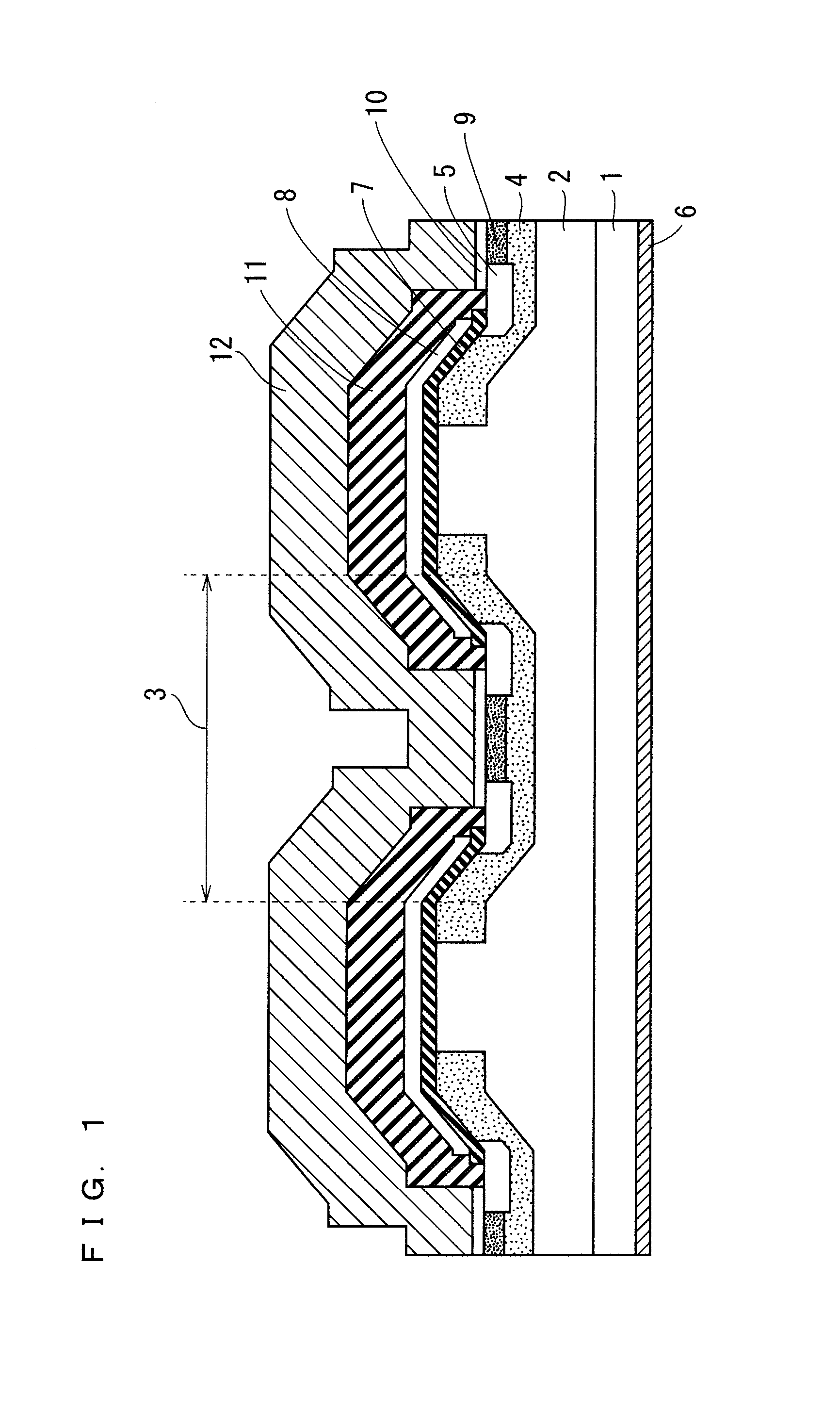
[0043]FIG. 1 is a diagram showing a cross-sectional structure of a silicon carbide semiconductor device in this embodiment of the present invention. FIG. 1 particularly shows two unit cells in a region (active region) through which current of the silicon carbide semiconductor device flows. An actual silicon carbide semiconductor device has a structure in which a plurality of the unit cells shown in FIG. 1 are repeatedly disposed in a horizontal direction and connected in parallel. A structure (termination structure) for relieving electric fields in a termination region is located around the active region, but it is not shown herein.
[0044]Herein, the above-mentioned silicon carbide (SiC) is a type of wide gap semiconductors. The wide gap semiconductors are typically semiconductors having a band gap of approximately 2 eV or more, and, for example, a group III nitride typified by gallium nitride (GaN), a group II oxide typified by zinc oxide (ZnO), a group II chalcogenide typifie...
second embodiment
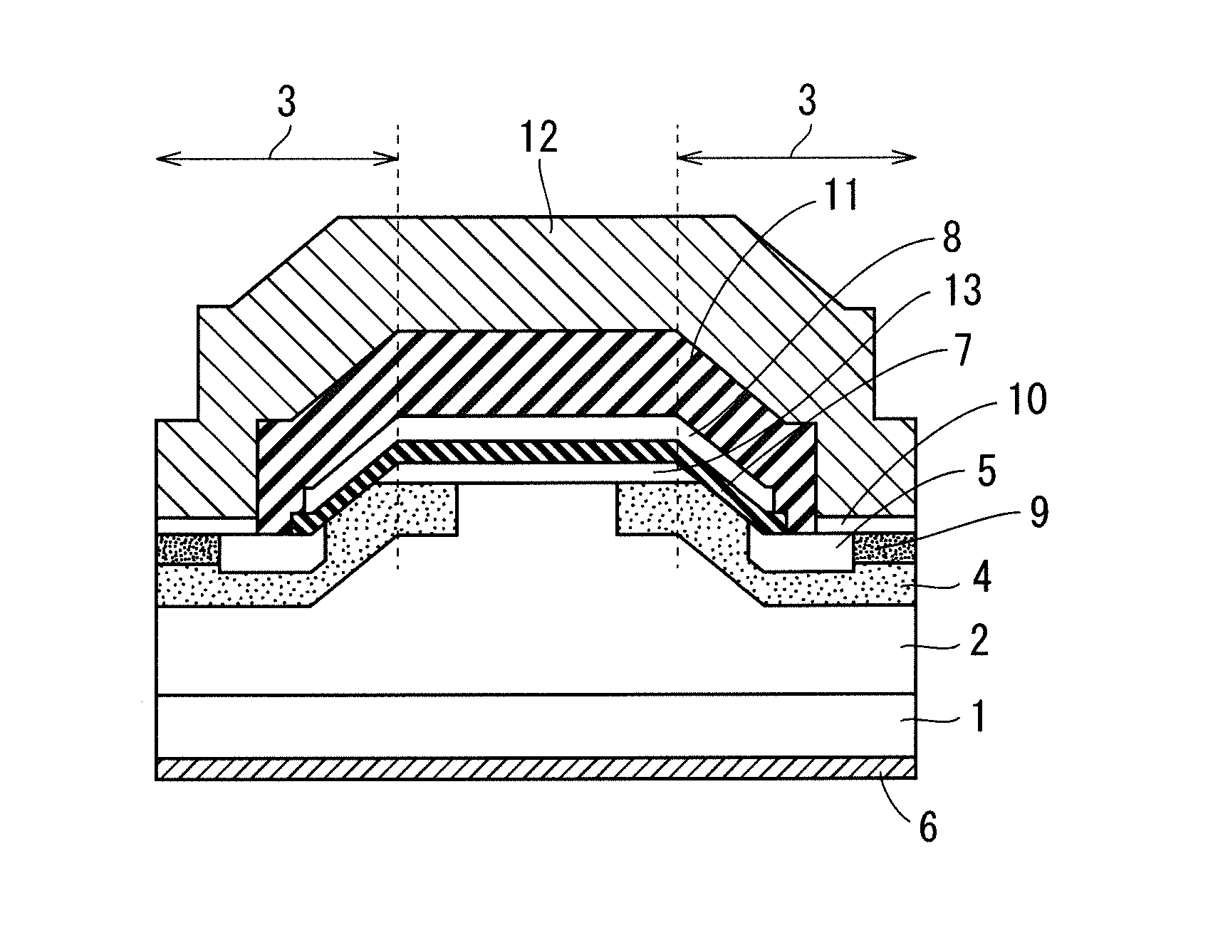
[0073]FIG. 2 is a diagram showing a cross-sectional structure of a silicon carbide semiconductor device in this embodiment of the present invention. Descriptions are given below with reference to the diagram showing one unit cell in the active region. The same configurations as the configurations shown in FIG. 1 are denoted by the same references, and detailed descriptions of the configurations are omitted.
[0074]As shown in FIG. 2, in the silicon carbide semiconductor device in this embodiment, a surface impurity layer 13 of the n-type is formed in the surface layer of the epitaxial layer 2 in the trench non-forming region and formed in the surface layer of the well layer 4 in the trench non-forming region. The surface impurity layer 13 is an n-layer containing impurities at a concentration higher than that of the epitaxial layer 2 of the n−-type. Then, the gate oxide film 7 is formed on the surface impurity layer 13, and furthermore, the gate electrode 8 is formed thereon.
[0075]The...
third embodiment
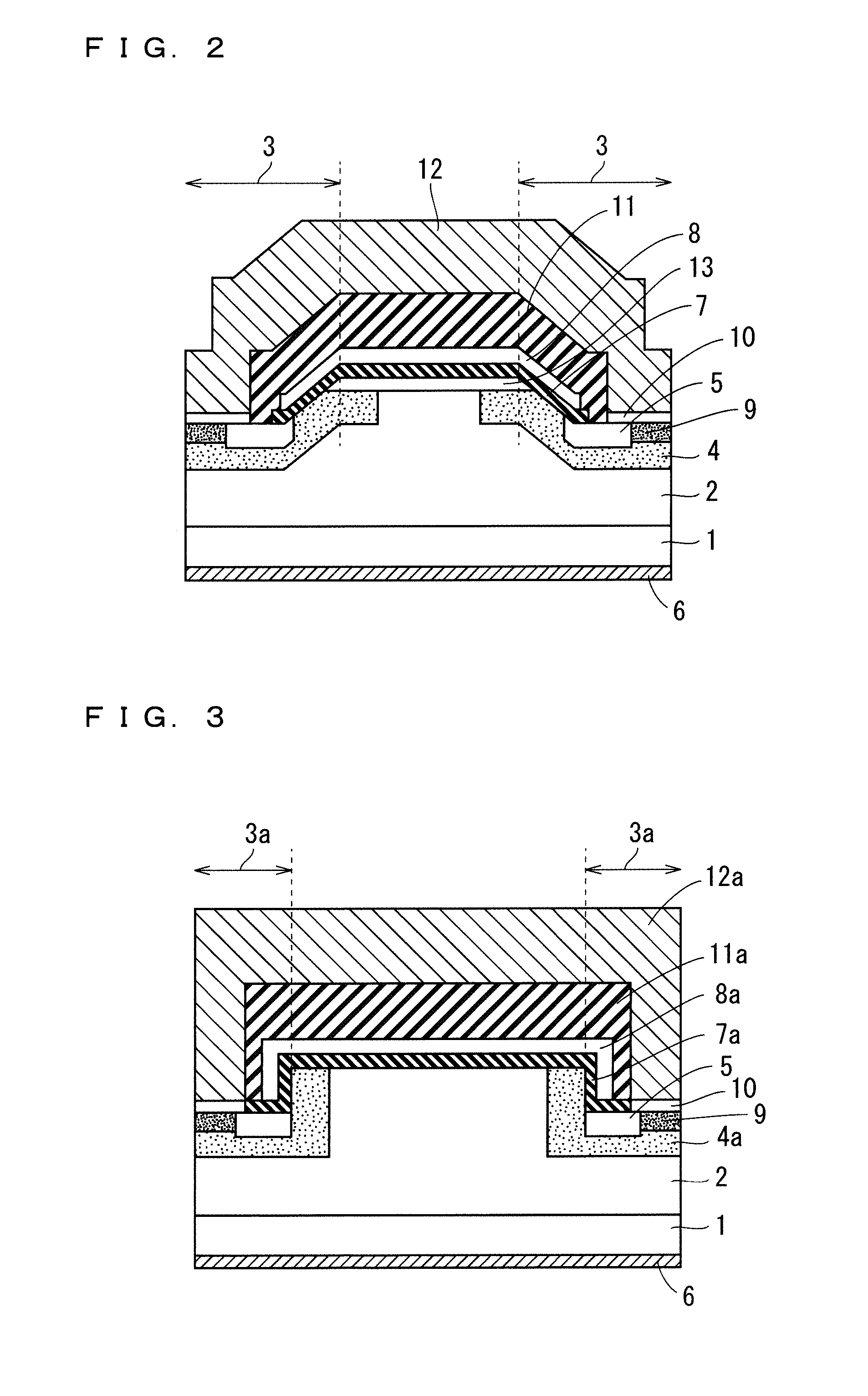
[0083]FIG. 3 is a diagram showing a cross-sectional structure of a silicon carbide semiconductor device in this embodiment of the present invention. The same configurations as the configurations shown in FIG. 1 are denoted by the same references, and detailed descriptions of the configurations are omitted.
[0084]As shown in FIG. 3, the silicon carbide semiconductor device in this embodiment includes the silicon carbide semiconductor substrate 1 of the n+-type and the epitaxial layer 2 of the n− silicon carbide epitaxially grown on the silicon carbide semiconductor substrate 1 of the n+-type, and a trench 3a is formed in the surface layer of the epitaxial layer 2. The trench 3a shown in FIG. 3 has side surfaces formed in a direction orthogonal to the surface of the epitaxial layer 2.
[0085]A well layer 4a of the p-type is formed in the surface layer of the epitaxial layer 2 in which the trench 3a is formed. In other words, the well layer 4a is formed along the bottom surface and the si...
PUM
 Abstract
Description
Claims
Application Information


