
Package structure

a packaging and structure technology, applied in the field of packaging structure, can solve the problems of difficult formation of patterned circuit layers, high cost of sputtering, complex manufacturing methods, etc., and achieve the effects of reducing the height-width ratio, enhancing bonding strength, and simplifying the manufacturing process of the package structur

Inactive Publication Date: 2016-08-11
IBIS INNOTECH
View PDF2 Cites 1 Cited by
  • Summary
  • Abstract
  • Description
  • Claims
  • Application Information

AI Technical Summary

Benefits of technology

The present invention is a package structure that uses a selective electroplating epoxy compound to create patterned circuit layers and conductive vias through an electroplating process. This simplifies the manufacturing process, reduces the overall thickness of the package, and allows for more flexible circuit design. Additionally, the conductive vias are designed with a lower segment and an upper segment connected by a minimal diameter difference, which improves bonding strength and prevents delamination between the two components.

Problems solved by technology

However, the processes in the manufacturing method are complicated and the cost of sputtering is relatively high.
Moreover, it is challenging for a patterned circuit layer formed by using a patterned dry film as an electroplating barrier to meet the requirement of fine pitch nowadays.
Moreover, the insulation layer is typically made of a polyimide or an Ajinomoto build-up film (ABF) resin, which costs higher.
Therefore, the package structures are currently manufactured in complicated processes with high cost.

Method used


Image

  • Package structure
  • Package structure
  • Package structure

Examples


Embodiment Construction

[0030]Reference will now be made in detail to the present preferred embodiments of the invention, examples of which are illustrated in the accompanying drawings. Wherever possible, the same reference numbers are used in the drawings and the description to refer to the same or like parts.

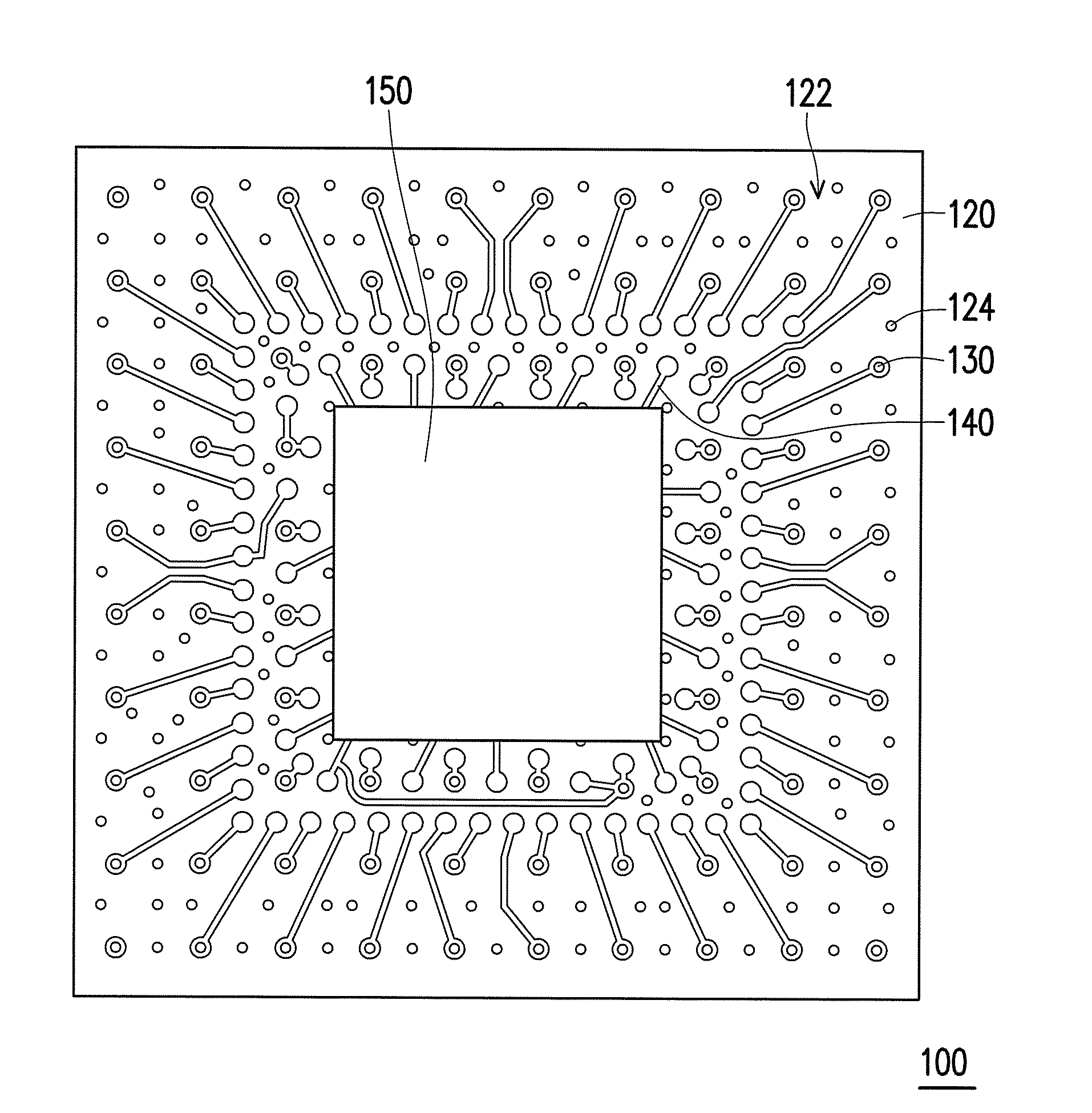
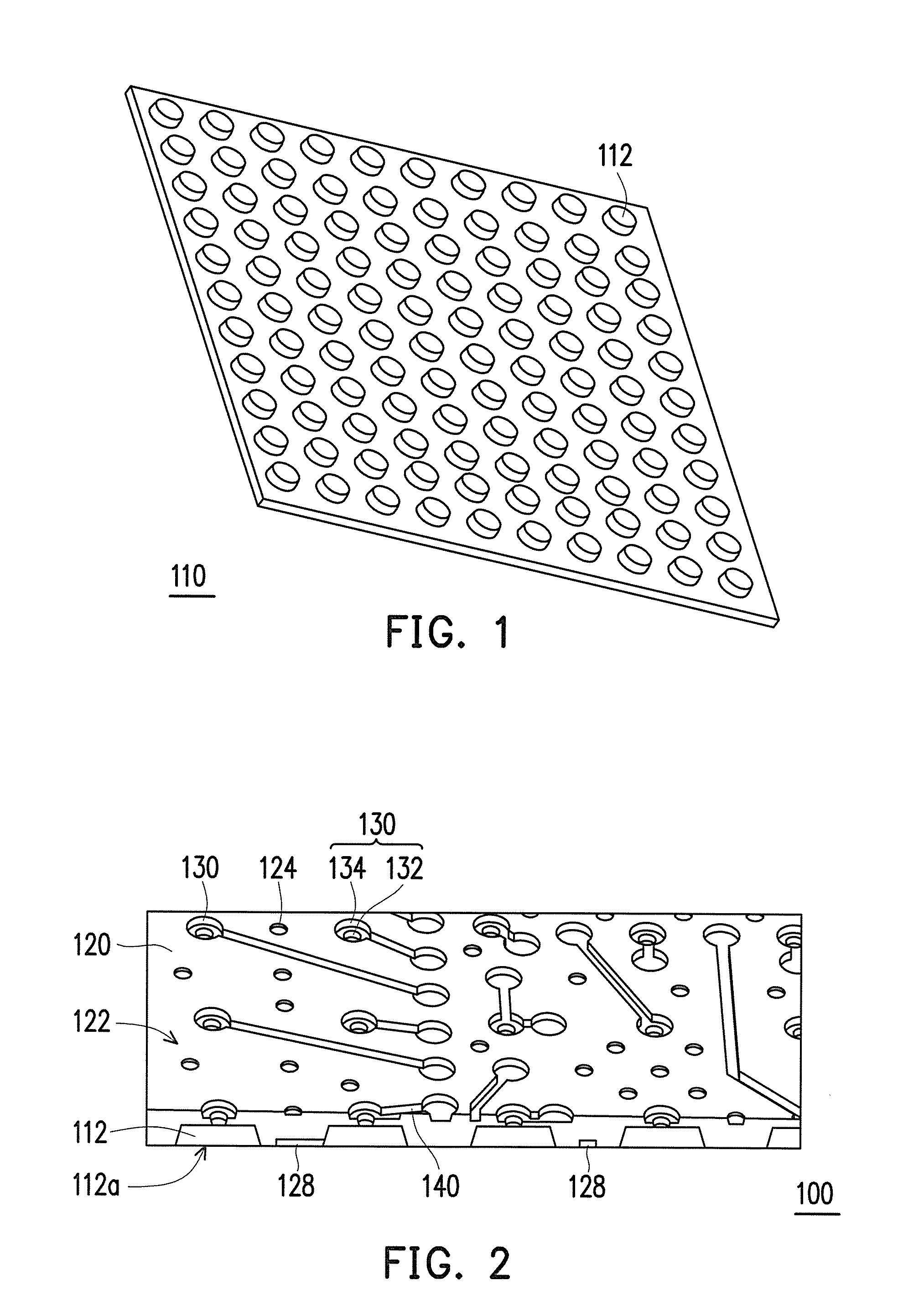
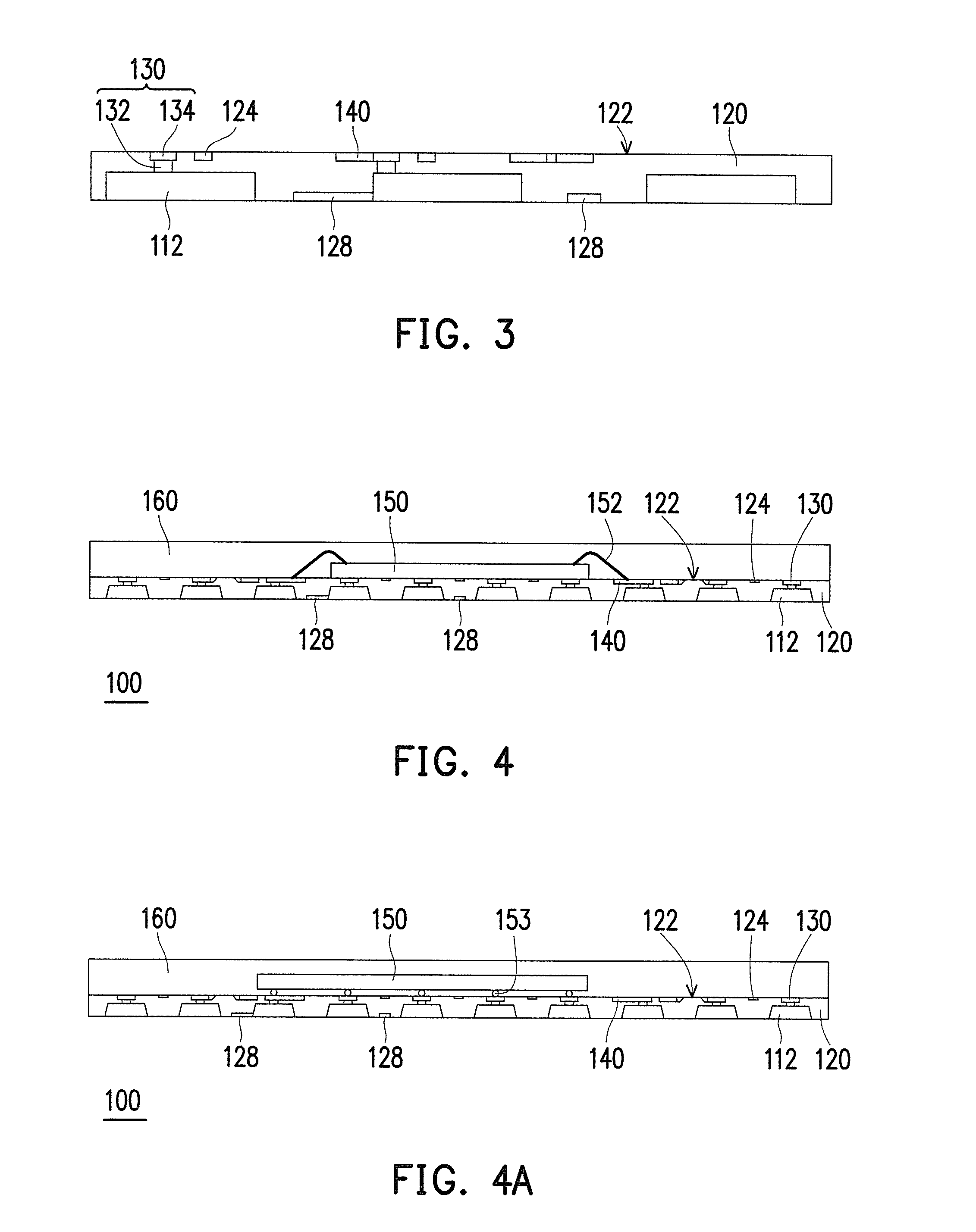
[0031]FIG. 1 is a schematic view of a lead frame according to an embodiment of the invention. FIG. 2 is a schematic view of a package structure according to an embodiment of the invention. FIG. 3 is a partial cross-sectional view of a package structure according to an embodiment of the invention. Referring to FIG. 1 to FIG. 3, the package structure 100 in the present embodiment includes a lead frame 110, a selective electroplating epoxy compound 120, a plurality of first conductive vias 130 and a first patterned circuit layer 140. The lead frame 110 as shown in FIG. 1 is firstly provided and includes a metal stud array having a plurality of metal studs 112 arranged in an array manner.

[0032]The lead f...


PUM


Abstract

A package structure includes a lead frame, a selective-electroplating epoxy compound, conductive vias and a patterned circuit layer. The lead frame includes a metal stud array having metal studs. The selective-electroplating epoxy compound covers the metal stud array. The selective-electroplating epoxy compound includes non-conductive metal complex. The conductive vias are directly embedded in the selective electroplating epoxy compound to be respectively connected to the metal studs and extended to a top surface of the selective-electroplating epoxy compound. Each of the conductive vias includes a lower segment connected to the corresponding metal stud and an upper segment connected to the lower segment and extended to the top surface, and a smallest diameter of the upper segment is greater than a largest diameter of the lower segment. The patterned circuit layer is directly disposed on the top surface and electrically connected to the conductive vias.

Description

CROSS-REFERENCE TO RELATED APPLICATION[0001]This application is a continuation-in-part application of and claims the priority benefit of U.S. application Ser. No. 14 / 663,447, filed on Mar. 19, 2015, now pending. The prior application Ser. No. 14 / 663,447 claims the priority benefit of Taiwan application serial no. 103121829, filed on Jun. 24, 2014. The entirety of each of the above-mentioned patent applications is hereby incorporated by reference herein and made a part of this specification.BACKGROUND OF THE INVENTION[0002]1. Field of the Invention[0003]The present invention generally relates to a package structure. More particularly, the present invention relates to a package structure capable of forming patterned circuit layers by directly electroplating a selective electroplating epoxy compound thereof.[0004]2. Description of Related Art[0005]In the information society nowadays, people tend to rely on electronic products more and more. To meet with the requirements of high speed, ...

Claims


Application Information

Patent Timeline
IPC IPC(8): H01L23/495H01L21/768
CPCH01L23/49586H05K2201/10674H01L23/4952H01L21/76825H01L21/76823H01L23/49558H05K1/0373H05K1/113H05K3/0014H05K3/105H05K3/188H05K3/4007H05K3/4697H05K2201/0236H05K2201/0376H05K2201/09063H05K2201/09118H05K2201/0919H05K2201/10151H05K2201/10515H01L23/49541H01L2924/181H01L2224/48091H01L23/13H01L23/49861H01L21/4828H01L2924/00014H01L2224/48247H01L2224/16245H01L2924/15153H01L24/16H01L24/48H01L2224/48227H01L2924/00012H01L2224/45099
Inventor LIU, WEN-CHUN
Owner IBIS INNOTECH
Learn More