Optical integrated circuit comprising light path turning micro-mirror inside the optical waveguide and method of manufacturing the same

a technology of integrated circuits and optical waveguides, applied in the direction of optical waveguide light guides, instruments, optics, etc., can solve the problems of large electrical signal attenuation, difficult mounting of chips themselves on a substrate, and complex alignment process between, so as to reduce optical power loss, improve quality, and reduce manufacturing costs

Active Publication Date: 2016-08-18
WOORIRO
View PDF3 Cites 9 Cited by
  • Summary
  • Abstract
  • Description
  • Claims
  • Application Information

AI Technical Summary

Benefits of technology

[0026]It is further an object of the present invention to provide an optical integrated circuit which reduces an optical power loss due to defects on a mirror surface by separately manufacturing the micro-mirror from optical integrated circuit manufacturing process and thereby providing a higher quality mirror surface, and a method of manufacturing the same.
[0027]In addition, the present invention is also related to an optical integrated circuit having a lower manufacturing cost by providing a light path turning micro-mirror made of various materials such as silicon, glass, and plastics, and a method of manufacturing the same.
[0029]A first sidewall of the groove which faces the slanted surface of the micro-mirror may be formed to be tilted at an angle in the range of 6° to 15° with respect to a longitudinal axis of the core layer to prevent re-entry of reflected light at the waveguide-air interface.

Problems solved by technology

In general, the photodetectors and VCSELs have very thin thickness of about 0.1 mm to 0.2 mm, therefore it is difficult to mount the chip itself on a substrate.
Those parallel optical coupling scheme between optical waveguides and active optical elements has several disadvantages: has a large volume, the end faces of the optical waveguides have to be polished, produces a large electrical signal attenuation caused by a long electrical connection path between the photodetector and an electrical signal processing element, and a complexity of alignment process between the photodetector and the optical waveguide.
Moreover, an electrical connection path between the photodetectors and signal processing devices can also be very short.
However, when the optical waveguide material is silica, it is very difficult to fabricate the above-described mirror surface 32 inside the optical waveguide because silica is known as a material very difficult to machine using dry etching techniques.
Such a particular features of the groove (30) used for the exemplified applications (U.S. Pat. No. 7,995,875 and 2014 / 0205234) make difficult to implement such grooves by using the conventional anisotropic dry etching techniques and even more with a single processing step.
In more detail, etching a groove having two different sidewall slopes as described above is very difficult.
However, most of the manufacturing methods proposed so far have several drawbacks; it requires very complex and high cost manufacturing processes such as electron-beam lithography, and in addition to that, the quality of the mirror surface and reproducibility of the slope angle are unsatisfactory.

Method used


Image

  • Optical integrated circuit comprising light path turning micro-mirror
inside the optical waveguide and method of manufacturing the same
  • Optical integrated circuit comprising light path turning micro-mirror
inside the optical waveguide and method of manufacturing the same
  • Optical integrated circuit comprising light path turning micro-mirror
inside the optical waveguide and method of manufacturing the same

Examples


Embodiment Construction

[0042]Hereinafter, an optical integrated circuit and a method of manufacturing the same according to exemplary embodiments of the present invention will be described in detail below with reference to the accompanying drawings. While the present invention is shown and described in connection with exemplary embodiments thereof, it will be apparent to those skilled in the art that various modifications can be made without departing from the spirit and scope of the invention.

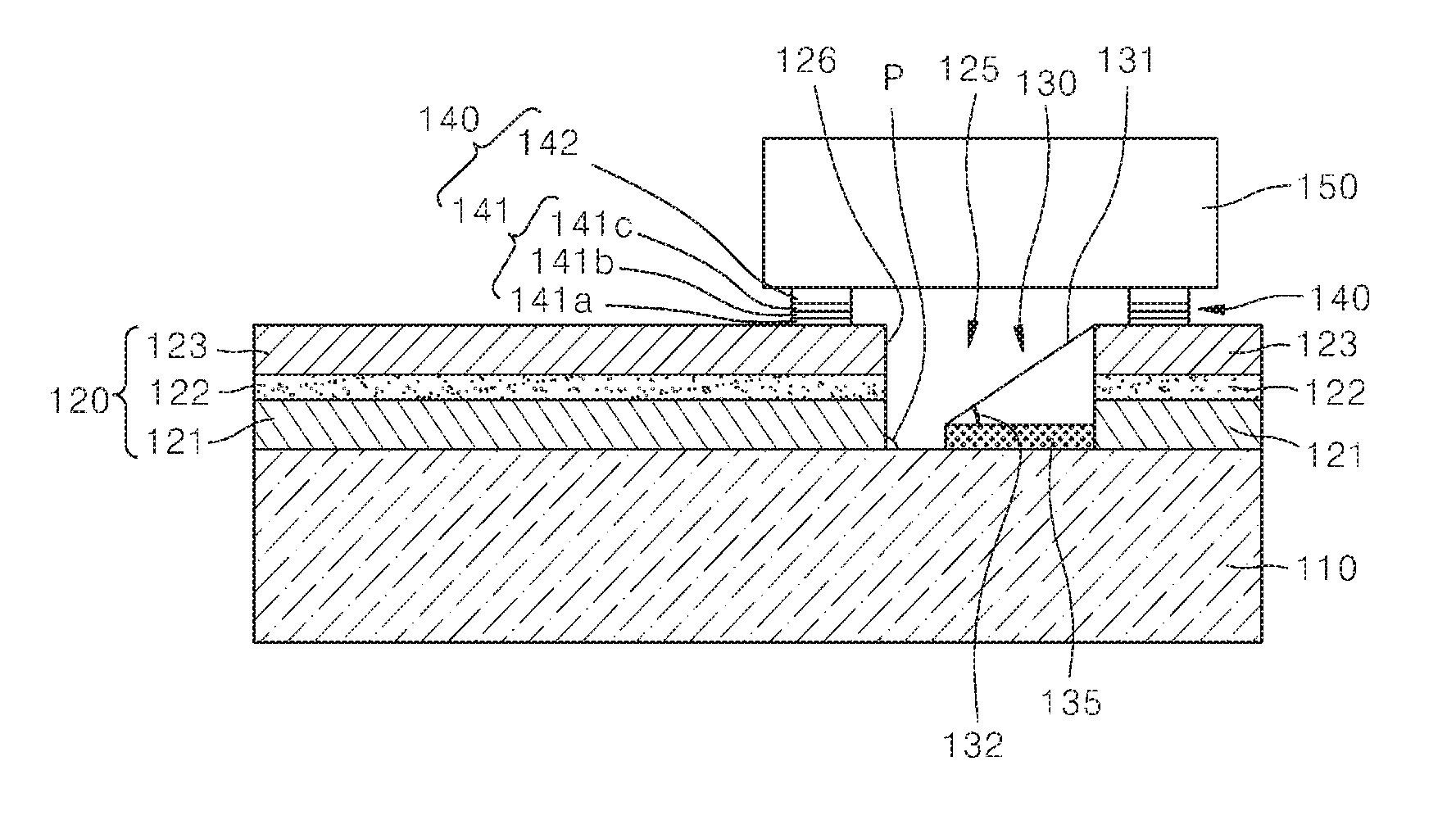
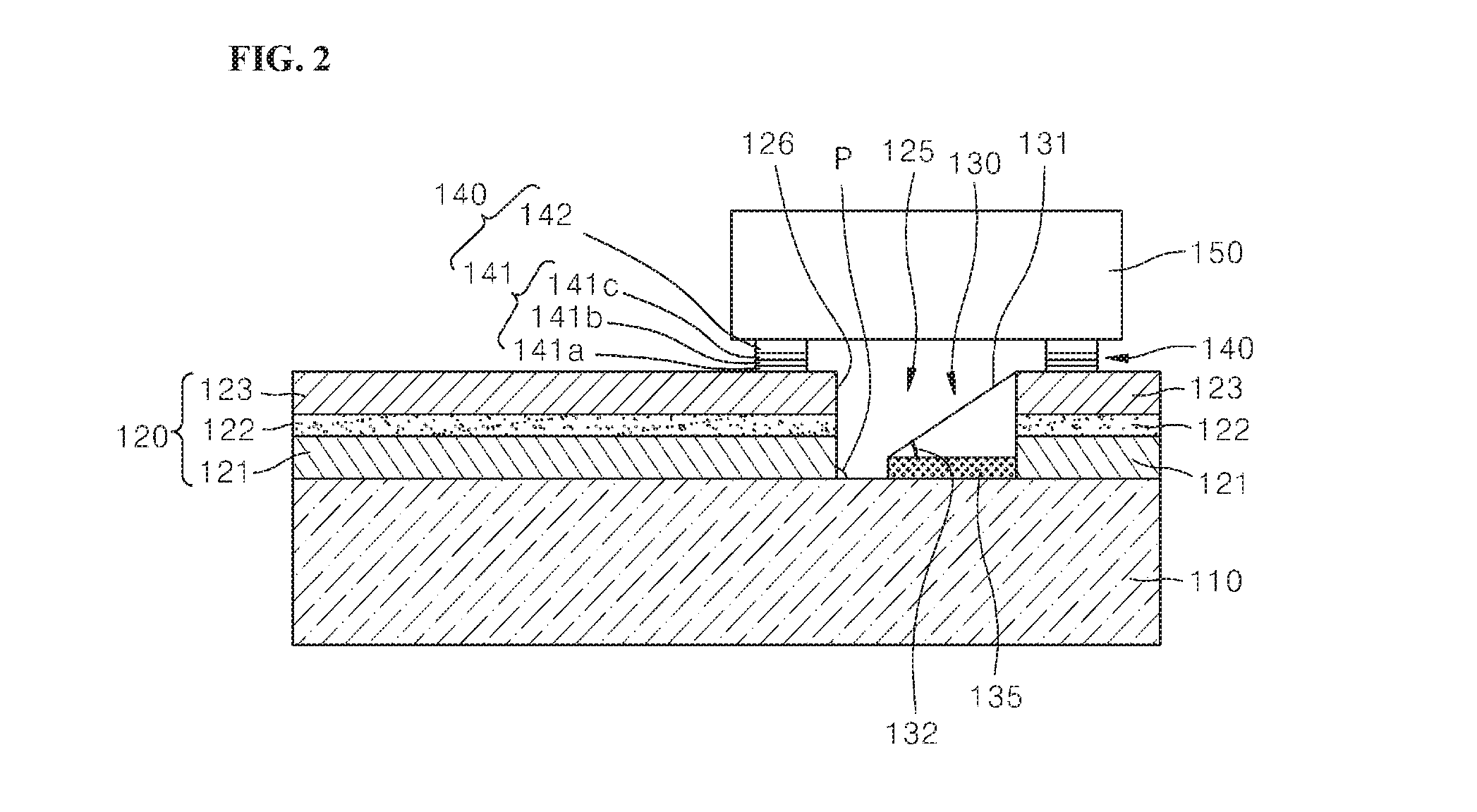
[0043]FIG. 2 is a cross-sectional view illustrating an optical integrated circuit according to a first embodiment of the present invention, and FIG. 3 is a plan view illustrating the optical integrated circuit shown in FIG. 2. For reference, an active optical element is indicated with a dotted line in FIG. 3.

[0044]Referring to FIGS. 2 and 3, an optical integrated circuit 100 according to the present invention comprises a substrate 110, an optical waveguide 120, a groove 125, a micro-mirror 130, bonding pads 140, and...


PUM


Abstract

An optical integrated circuit comprises optical waveguides formed by sequentially stacking a lower cladding layer, a core layer and a upper cladding layer on a substrate, grooves formed by etching the upper cladding layer, the core layer and all or parts of the lower cladding layer close to a end section of the optical waveguide to intercept light transmitted through the core layer of the optical waveguide or to couple light into the core layer, a plurality of bonding pads formed around the groove, micro-mirrors which is inserted into the grooves and cemented thereinto, and have at least one slanted side surface inclined in a range of 30° to 60° with respect to the bottom surface to reflect a light which exits horizontally from the core layer to the groove and turn the path of the exited light vertically toward the upper side of the groove or conversely to reflect light which emitted vertically from an upper side of the groove and turn the path of the emitted light horizontally to couple into the core layer, and active optical elements bonded over the grooves by bonding pads and emits light toward the slanted surface of the micro-mirror or conversely, receives light reflected by the micro-mirror. Such a PLC based optical integrated circuit and a method of manufacturing the same provides a low-cost manufacturing of optical integrated circuits and high quality mirrors for vertical optical coupling scheme.

Description

RELATED APPLICATION[0001]This application claims the benefit of priority of Korean Patent Application No. 10-2015-0022625 filed Feb. 13, 2015, the contents of which are incorporated herein by reference in their entirety.FIELD AND BACKGROUND OF THE INVENTION[0002]1. Field of the Invention[0003]The present invention relates to an optical integrated circuit and a method of manufacturing the same. More particularly it relates to a PLC based optical integrated circuit including a light path turning micro-mirror inside the optical waveguide and a method of the same.[0004]2. Description of the Related Art[0005]The transmission capacity of optical communication system and optical interconnection apparatus has been continuously increased to meet the rising demand of wired / wireless communication traffic. A transmission distance of an optical cable decreases as data rate increases same as a copper cable. Accordingly new transmission technologies such as a multi lane transmission techniques and...

Claims


Application Information

Patent Timeline
Patent Type & Authority Applications(United States)
IPC IPC(8): G02B6/42G02B6/136G02B6/12
CPCG02B6/4214G02B6/12004G02B2006/12038G02B2006/121G02B2006/12061G02B6/136G02B6/125G02B6/43
Inventor LEE, SANG HWANPARK, CHAN YONGKIM, YOUNG HYE
Owner WOORIRO
Why Eureka
Try Eureka