Method of forming a semiconductor structure

a technology of semiconductor structure and fin-shaped structure, which is applied in the direction of semiconductor device, semiconductor/solid-state device testing/measurement, electrical apparatus, etc., can solve the problems of extreme challenges, physical limitations and various processing parameters, and the shrinkage of the width of each fin-shaped structure, so as to achieve the required demands and form fin-shaped structures. , to achieve the effect of achieving the required demands

Active Publication Date: 2016-08-25
MARLIN SEMICON LTD
View PDF3 Cites 19 Cited by
  • Summary
  • Abstract
  • Description
  • Claims
  • Application Information

AI Technical Summary

Benefits of technology

[0006]It is one of the primary objectives of the present invention to provide a method of forming a semiconductor structure, in which the critical dimensions (CD) of the mandrels or spacers are allowed for timely adjusting during the SIT process, so as to obtain the fin-shape structure with accurate fin size and pitch.
[0008]In the method of forming a semiconductor structure of the present invention, the critical dimension of the mandrel patterns is controlled via timely checking and adjusting a width of each mandrel and each spacer in the SIT process. Thus, through the method of forming a semiconductor structure, it is sufficient to obtain fine fin-structure free from pitch walking issues.

Problems solved by technology

However, with the demands of miniaturizing the semiconductor devices, the width of each fin-shaped structure, as well as the spacing therebetween both shrinks dramatically.
Thus, forming fin-shaped structures which can achieve the required demands under the restrictions of miniaturization, physical limitations and various processing parameters becomes an extreme challenge.

Method used


Image

  • Method of forming a semiconductor structure
  • Method of forming a semiconductor structure
  • Method of forming a semiconductor structure

Examples


first embodiment

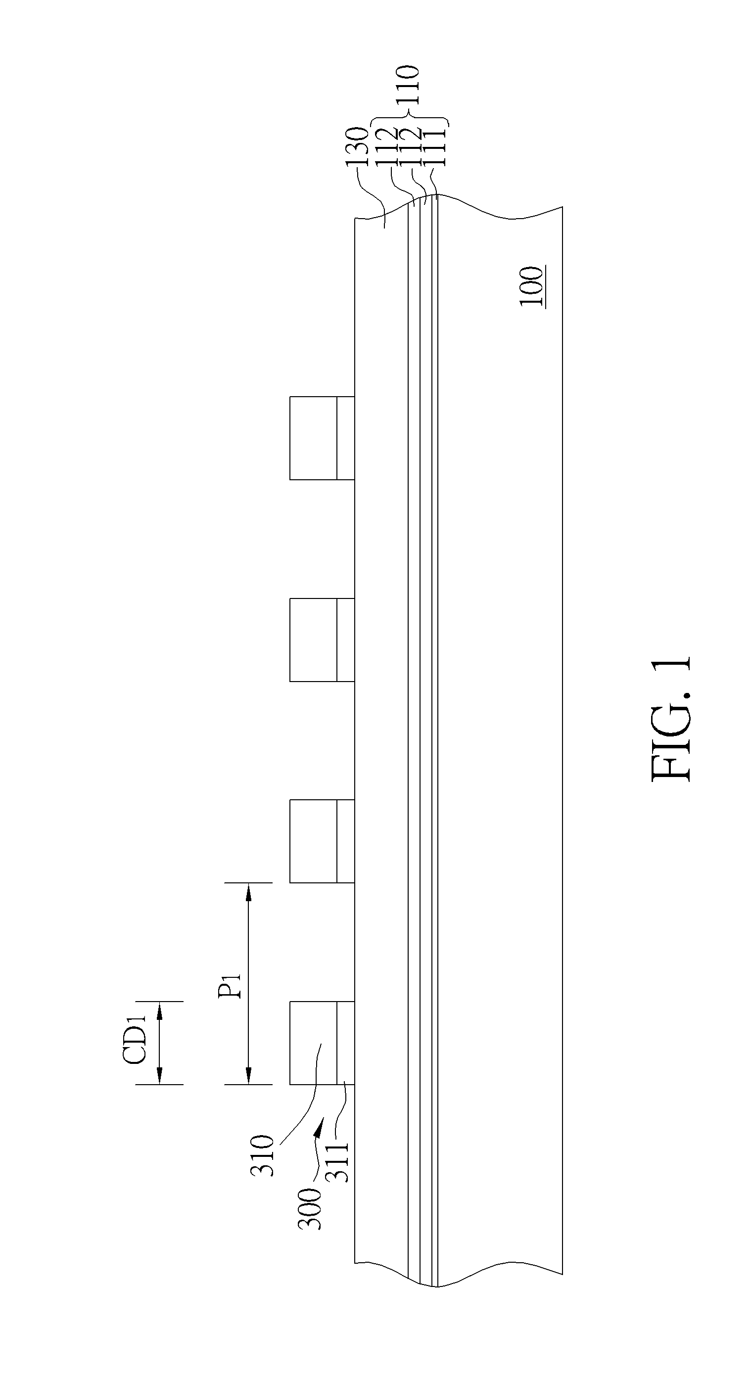
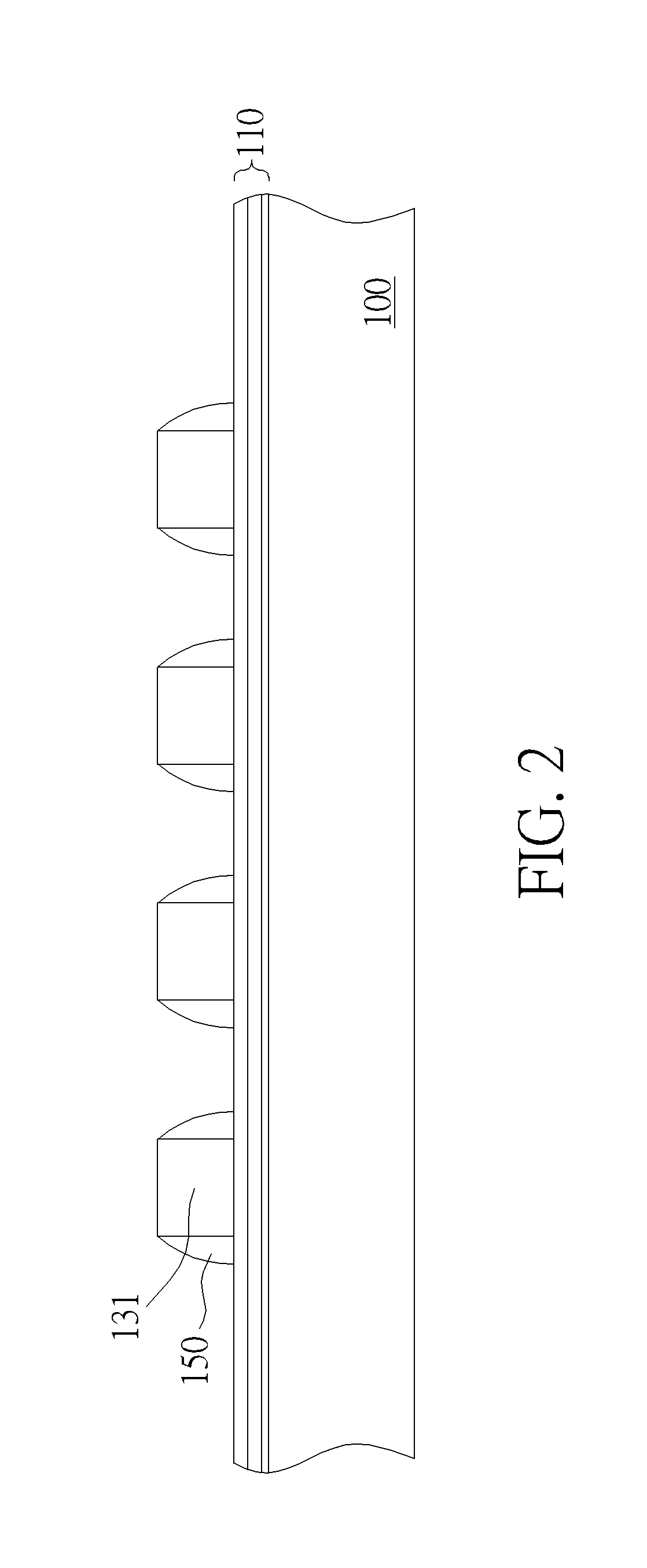
[0017]Please refer to FIGS. 1-4, which illustrate a method of forming a semiconductor structure in accordance with the present invention. First of all, as shown in FIG. 1, a substrate 100 is provided, and a first hard mask layer 110, a second hard mask layer 130 and a photoresist layer 300 are formed sequentially on the substrate 100 from bottom to top. Precisely speaking, the substrate 100 for example is a semiconductor substrate, including silicon substrate, silicon germanium substrate, silicon carbide substrate, or silicon on insulator (SOI). The first hard mask layer 110 and the second hard mask layer 130 are entirely formed on a top surface of the substrate 100, for example, through a chemical vapor deposition (CVD) process or a physical vapor deposition (PVD) process, wherein the first hard mask layer 110 and the second hard mask layer 130 may include a monolayer structure or a multi-layer structure including oxide layer or a nitride layer. In one embodiment of the present inv...

second embodiment

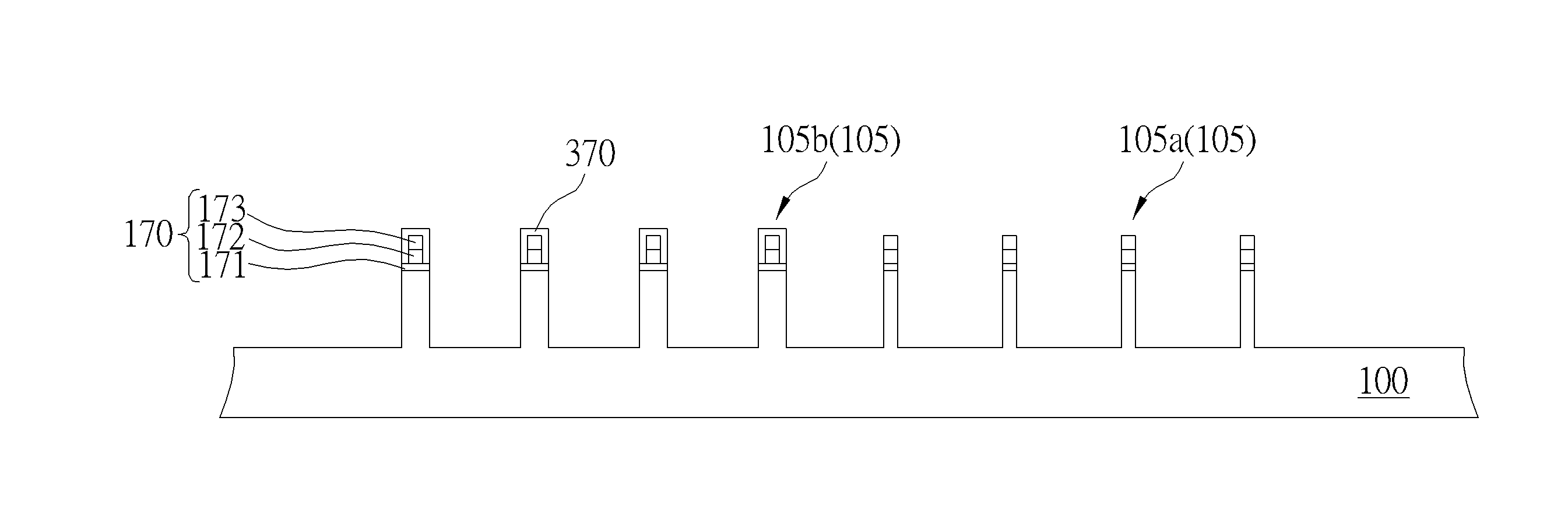
[0036]Thus, through the aforementioned steps, the semiconductor structure of the second embodiment may be obtained. After these, an insulation layer (not shown in the drawings) may be formed on the semiconductor structure between the fins 103 to configure as shallow trench isolation (STI; not shown in the drawings), and a gate structure (not shown in the drawings) may be further formed across the fin shaped structures, for example, after the third mask layer 170 is removed, to serve as a multi-gate structure.

[0037]It is worth mentioning that, the method of the present invention may also be used on a dSIT process to form the fins 103 having substantially the same width critical dimension approaching ⅕ to ⅛ of the aforementioned critical dimension CD1, preferably around 10 nanometers or less. It is also known that, the present invention repeatedly checks and timely adjusts the critical dimension of each mandrel (including first mandrels and second mandrels) and each spacer (including ...

third embodiment

[0040]Then, as shown in FIG. 17, the pattern of the third mandrels 175 and the fourth mandrels 178 are simultaneously transferred to the fourth layer 171 and the substrate 100 underneath, to form a plurality of fins 105, for example through an etching process which is known by person in the arts and will not be redundantly described. It is worth mentioning that, since the fins 105 are formed by using the third mandrels 175 and the fourth mandrels 178 to serve as hard masks, the fins 105 may include first fins 105a and second fins 105b having different widths (also known as different critical dimensions). However, the method of the third embodiment is not limited to the above-mentioned steps, but may include other processes. For example, in other embodiments, the masking layer may be optionally formed after covering the portion of the third mandrels with the sacrificial mask layer, or the masking layer is omitted and an additional etching process may be carried out after covering the...


PUM

PropertyMeasurementUnit
semiconductor structureaaaaaaaaaa
critical dimensionaaaaaaaaaa
widthaaaaaaaaaa

Abstract

A method of forming a semiconductor structure includes following steps. First of all, a patterned hard mask layer having a plurality of mandrel patterns is provided. Next, a plurality of first mandrels is formed on a substrate through the patterned hard mask. Following these, at least one sidewall image transferring (SIT) process is performed. Finally, a plurality of fins is formed in the substrate, wherein each of the fins has a predetermined critical dimension (CD), and each of the mandrel patterns has a CD being 5-8 times greater than the predetermined CD.

Description

BACKGROUND OF THE INVENTION[0001]1. Field of the Invention[0002]The present invention relates to a method of forming a semiconductor structure, and more particularly to a method of forming a semiconductor structure which can tune pitch walking issues.[0003]2. Description of the Prior Art[0004]With increasing miniaturization of semiconductor devices, various multi-gate MOSFET devices have been developed. The multi-gate MOSFET is advantageous for the following reasons. First of all, the fabrication of the multi-gate MOSFET devices is allowable to be integrated into traditional logic device processes, and thus is more compatible. In addition, since the three-dimensional structure of the multi-gate MOSFET increases the overlapping area between the gate and the substrate, the channel region is controlled more effectively, thereby reducing both the drain-induced barrier lowering (DIBL) effect and the short channel effect. Moreover, as the channel region is longer for the same gate length,...

Claims


Application Information

Patent Timeline
Patent Type & Authority Applications(United States)
IPC IPC(8): H01L21/033H01L21/66
CPCH01L21/0337H01L22/12H01L21/0338H01L21/3086H01L21/3088H01L29/66795H01L21/823431H01L21/3083
Inventor FENG, LI-WEITSAI, SHIH-HUNGLIN, CHAO-HUNGLIU, HON-HUEILIU, AN-CHIWU, CHIH-WEIJENQ, JYH-SHYANGHONG, SHIH-FANGLIOU, EN-CHIUANFU, SSU-IHUNG, YU-HSIANGHSU, CHIH-KAICHEN, MEI-CHENTSENG, CHIA-HSUN
Owner MARLIN SEMICON LTD
Why Eureka
Try Eureka