Methods for fabricating integrated circuits using directed self-assembly including a substantially periodic array of topographical features that includes etch resistant topographical features for transferability control

Active Publication Date: 2016-08-25
GLOBALFOUNDRIES US INC
View PDF3 Cites 3 Cited by
  • Summary
  • Abstract
  • Description
  • Claims
  • Application Information

AI Technical Summary

Benefits of technology

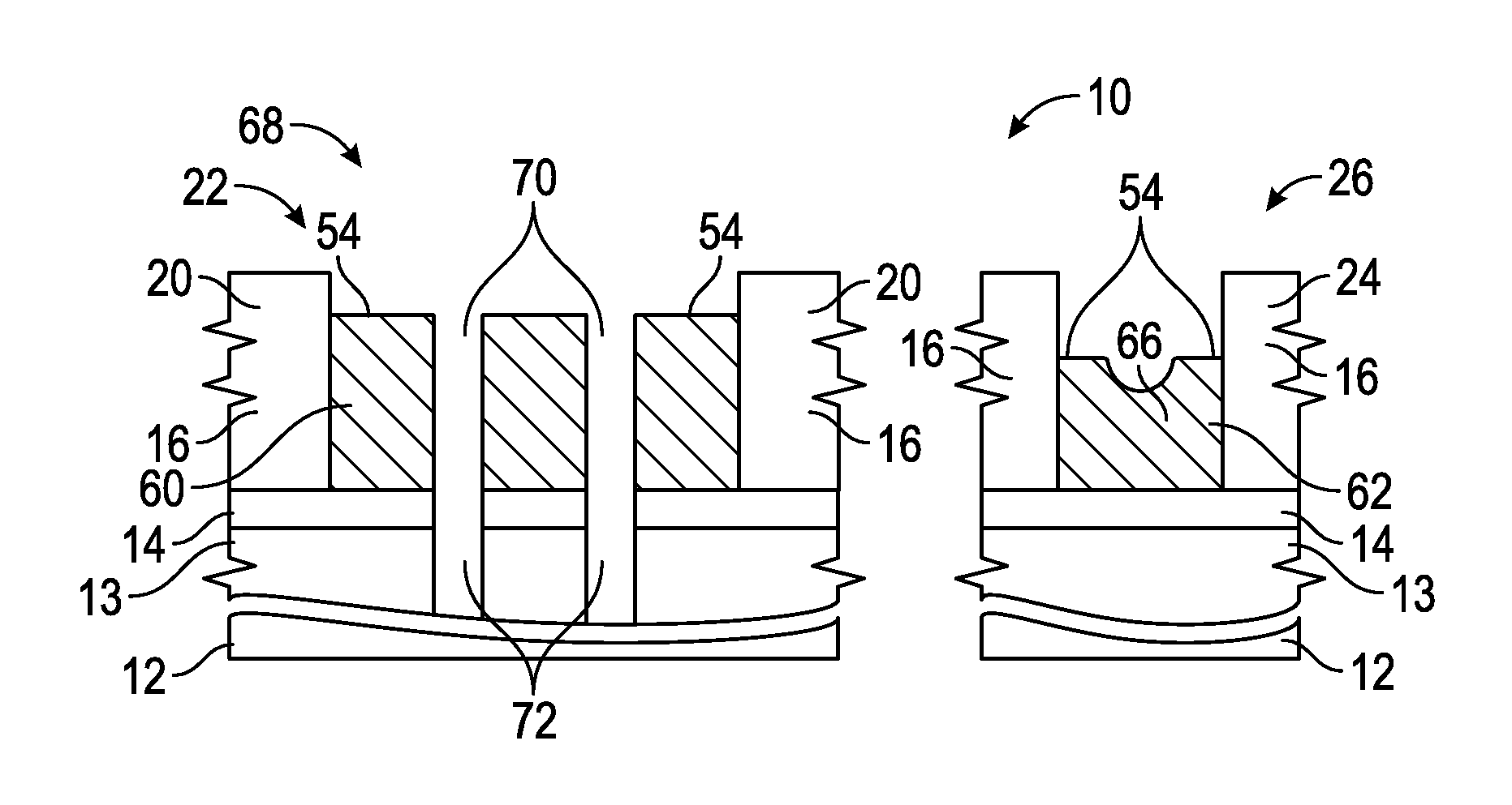
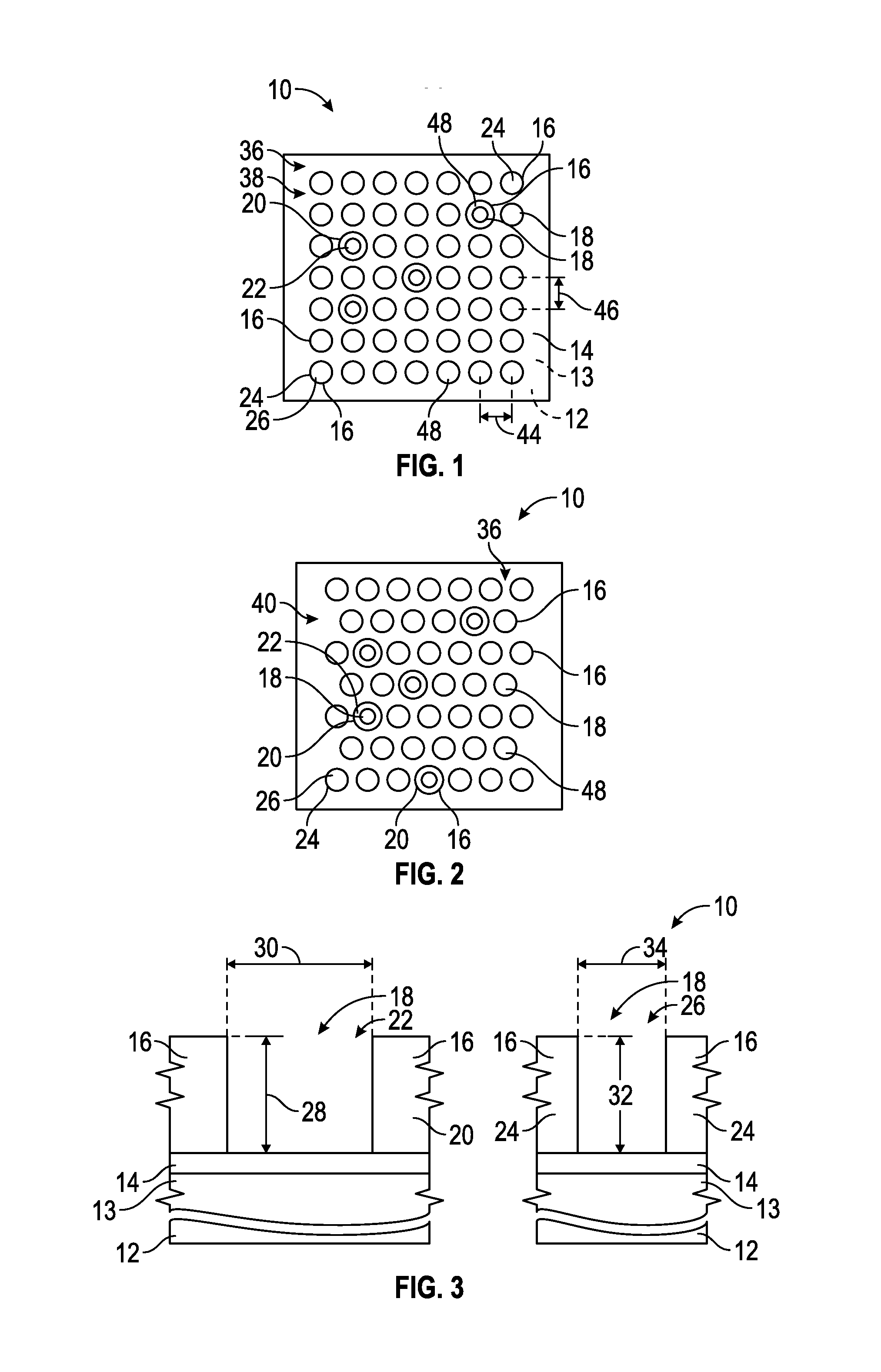
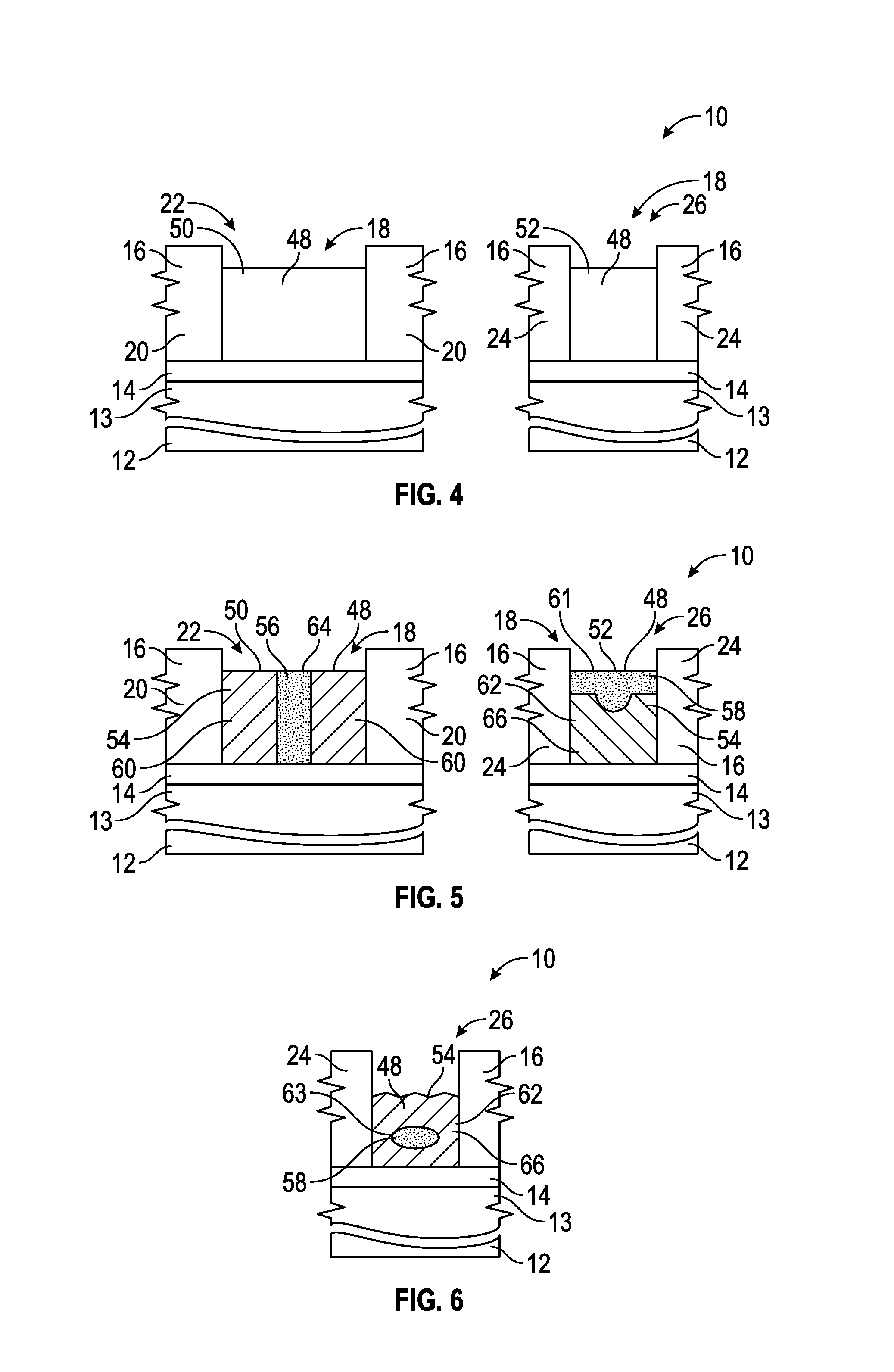
This patent describes methods for fabricating integrated circuits using a process called directed self-assembly (DSA). The methods involve creating a pattern of topographical features on a semiconductor substrate, which include etch resistant features and graphoepitaxy features. The etch resistant features create shallow wells that hold a block copolymer, while the graphoepitaxy features create deeper wells that hold a different block copolymer. The block copolymer is then separated into two phases, and the etch resistant features direct the first phase to form plugs in the shallow wells, while the graphoepitaxy features direct the second phase to extend through the deeper wells. This process allows for precise placement of components in the integrated circuit.

Problems solved by technology

Whilst double and other multi-patterning processes can realize smaller pitch, these approaches are expensive and more complex.
Unfortunately, current techniques for forming DSA patterns can have considerable process variations that reduce the DSA process window (DSAPW) including reducing transferability control of the topographical features for DSA.
The size of these non-printing lithographic assist features is relatively small such that they do not print or transfer to the photoresist layer and otherwise produce unintended features in the integrated circuit.
Unfortunately, the relatively small size of these non-printing lithographic assist features limits their benefit for improving the lithographic process window.
In the lower density areas, the confinement wells are particularly susceptible to overfilling with the BCP.
However, this may be undesirable because the artificially added confinement wells will generally result in additional features in the mask that will be etch transferred to the underlying substrate resulting, for example, in unintended electrical connections between layers of the substrate.

Method used


Image

  • Methods for fabricating integrated circuits using directed self-assembly including a substantially periodic array of topographical features that includes etch resistant topographical features for transferability control
  • Methods for fabricating integrated circuits using directed self-assembly including a substantially periodic array of topographical features that includes etch resistant topographical features for transferability control
  • Methods for fabricating integrated circuits using directed self-assembly including a substantially periodic array of topographical features that includes etch resistant topographical features for transferability control

Examples


example

[0048]FIG. 15 is an example of computational simulations for determining the dimensions of topographical features and corresponding confinement wells in accordance with an exemplary embodiment. The example is provided for illustration purposes only and is not meant to limit the various embodiments in any way.

[0049]To simulate graphoepitaxy DSA patterns, a masking method referenced in Exploration of the Directed Self-Assembly Based Nano-Fabrication Design Space Using Computational Simulations by Azat Latypov et al., which is incorporated herein in its entirety, is used to model confinement of block copolymers in a three-dimensional simulation domain. The BCP used for the simulation was PS-b-PMMA with a volume fraction of a PS phase of f=0.7, a degree of polymerization of N=663, and an unperturbed radius of gyration of Rg=10 nm. The depth of the confinement wells 18a-h was set to 50 nm and the widths of the confinement wells 18a-h were varied from 55 to 90 nm. As illustrated, the conf...


PUM


Abstract

Methods for fabricating integrated circuits are provided. In one example, a method for fabricating an integrated circuit includes forming a substantially periodic array of a plurality of topographical features including a plurality of etch resistant topographical features and at least one graphoepitaxy feature. The plurality of etch resistant topographical features define a plurality of etch resistant confinement wells and the at least one graphoepitaxy feature defines a graphoepitaxy confinement well that has a different size and / or shape than the etch resistant confinement wells. A block copolymer is deposited into the confinement wells. The block copolymer is phase separated into an etchable phase and an etch resistant phase. The etch resistant topographical features direct the etch resistant phase to form an etch resistant plug in each of the etch resistant confinement wells.

Description

TECHNICAL FIELD[0001]The technical field relates generally to methods for fabricating integrated circuits, and more particularly relates to methods for fabricating integrated circuits including topographical features for directed self-assembly.BACKGROUND[0002]Decreasing device size and increasing device density has traditionally been a high priority for the manufacturing of integrated circuits. Optical lithography has been the driving force for device scaling. Conventional optical lithography is limited to about 80 nm pitch for single exposure patterning. Whilst double and other multi-patterning processes can realize smaller pitch, these approaches are expensive and more complex.[0003]Directed self-assembly (DSA), a technique which aligns self-assembling polymeric materials on a lithographically defined guide pattern, is a potential option for extending current optical lithography beyond its pitch and resolution limits. The self-assembling materials, for example, are block copolymer...

Claims


Application Information

Patent Timeline
IPC IPC(8): H01L21/308
CPCH01L21/3086H01L21/0271G03F7/0002
Inventor LATYPOV, AZATCOSKUN, TAMERPREIL, MOSHE
Owner GLOBALFOUNDRIES US INC
Why Eureka
Try Eureka