Ferroelectric device and meethod for manufacturing same

a technology of ferroelectric devices and meethods, which is applied in the direction of solid-state devices, chemical vapor deposition coatings, coatings, etc., can solve the problems of inability to retain data, data written on the device when seen to operate as a memory transistor does the data written on the device when seen to operate as a memory transistor does not disappear in one day at the longest after writing, etc., to achieve the effect of a

Active Publication Date: 2016-08-25
NAT INST OF ADVANCED IND SCI & TECH +1
View PDF6 Cites 13 Cited by
  • Summary
  • Abstract
  • Description
  • Claims
  • Application Information

AI Technical Summary

Benefits of technology

[0060]According to the present invention, it can be implemented and realized to write and to read data with a single transistor size. Moreover, the data written is not to disappear, for a practically sufficiently long time.
[0061]And, data read out is not to be destroyed in contents. A ferroelectric device according to the present invention can be used in a variety of circuit such as for a semiconductor memory in a wide range of applications, and further for a temporary storage device and the like that is stable in a semiconductor logic circuit. According to the present invention, furthermore, ferroelectric devices if micronized are to have wider memory windows achieved.
[0062]A ferroelectric device according to the present invention is especially effective and significant with a gate stack small in volume. To wit, while if the gate length is 200 nm or less, the data retention time period has hitherto been shortened and the memory window narrowed, it has been found that a ferroelectric device according to the invention can exhibit a wider memory window for a prolonged period of time.
[0063]With a gate stack formed on its side faces with a lateral wall layer constituted of a second ferroelectric identical in composition to the first ferroele...

Problems solved by technology

Conventional MFS and MFIS transistors have had the problem, however, that data written on them when seen to operate as a memory transistor do disappear in one day at the longest after writing (see Non-patent References 1 and 2).
To wit, for those conventional MFS and MFIS transistors it was not possible to retain data for a term which their implementation requires.
This is believed to be mainly due to large leakage currents through the buffer layer and ferroelectric, causing cha...

Method used


Image

  • Ferroelectric device and meethod for manufacturing same
  • Ferroelectric device and meethod for manufacturing same
  • Ferroelectric device and meethod for manufacturing same

Examples


embodiments

Example 1

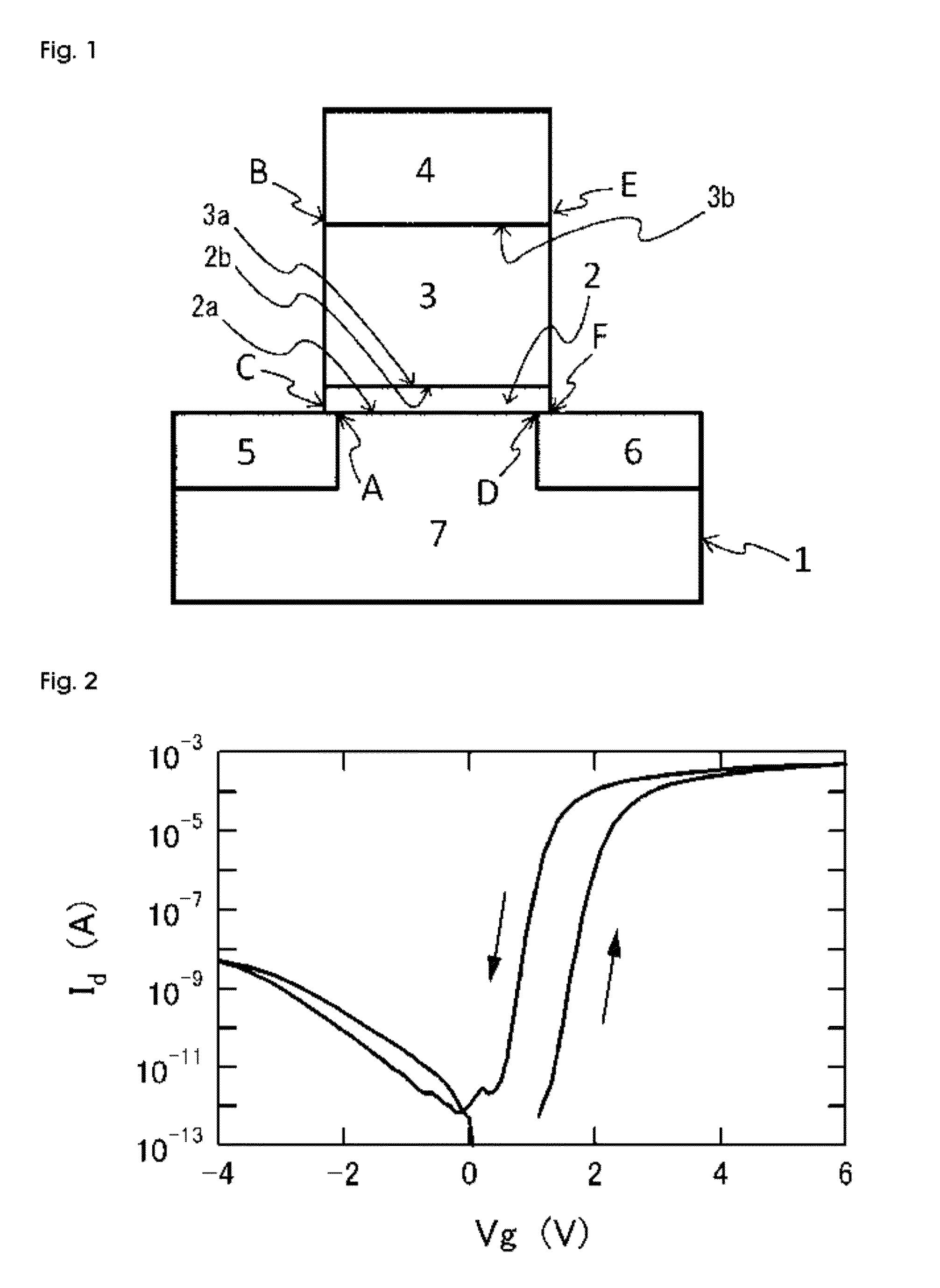
[0257]In Example 1 as an embodiment of the present invention, a transistor structured as shown in FIG. 1 is made.

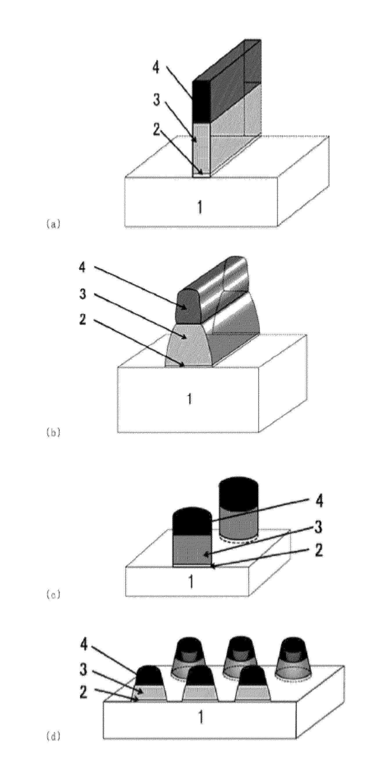
[0258]Materials used, thicknesses and others are as follows:[0259]Semiconductor 1 constituted by a Si substrate having a source and a drain region preformed.[0260]Insulator 2 composed of HfO2, and having a thickness of 7 nm.[0261]First Ferroelectric, i.e. Ferroelectric 3 composed of SCBT and having a thickness of 200 nm[0262]Conductor 4 composed of Pt and having a thickness of 200 nm.[0263]Gate length (length of gate metal from the source region towards the drain region) of 10 μm[0264]Type of conduction of the source and drain regions 5 and 6: n type[0265]Type of conduction of region 7: p type

[0266]HfO2 is formed as built up by pulse laser deposition. The laser used is KrF excimer laser. Laser excimer is of 250 mJ per pulse and a repetition frequency of pulses: 2 Hz. The substrate has a temperature of 220° C. Gas introduced into a build-up chamber is nitrogen gas...

example 2

[0283]In Example 2, rates of flow of MOCVD liquid materials different from those in Example 1 are adopted. Also, the period of heat treatment for crystallization is altered. Other conditions are identical to those in Example 1. To wit:

[0284]Liquid Raw Materials

[0285]ST-1 (concentration of 0.1 M): 0.106 sccm

[0286]CT-1 (concentration of 0.1 M): 0.049 sccm

[0287]Bi (MMP)3: (concentration of 0.2 M): 0.146 sccm

[0288]PET (concentration of 0.1 M): 0.038 sccm

[0289]Film Forming Time Period: 1457 seconds

[0290]Heat Treatment Conditions: heat treatment in oxygen under the atmospheric pressure, at a temperature of 800° C. and for a time period of 60 minutes.

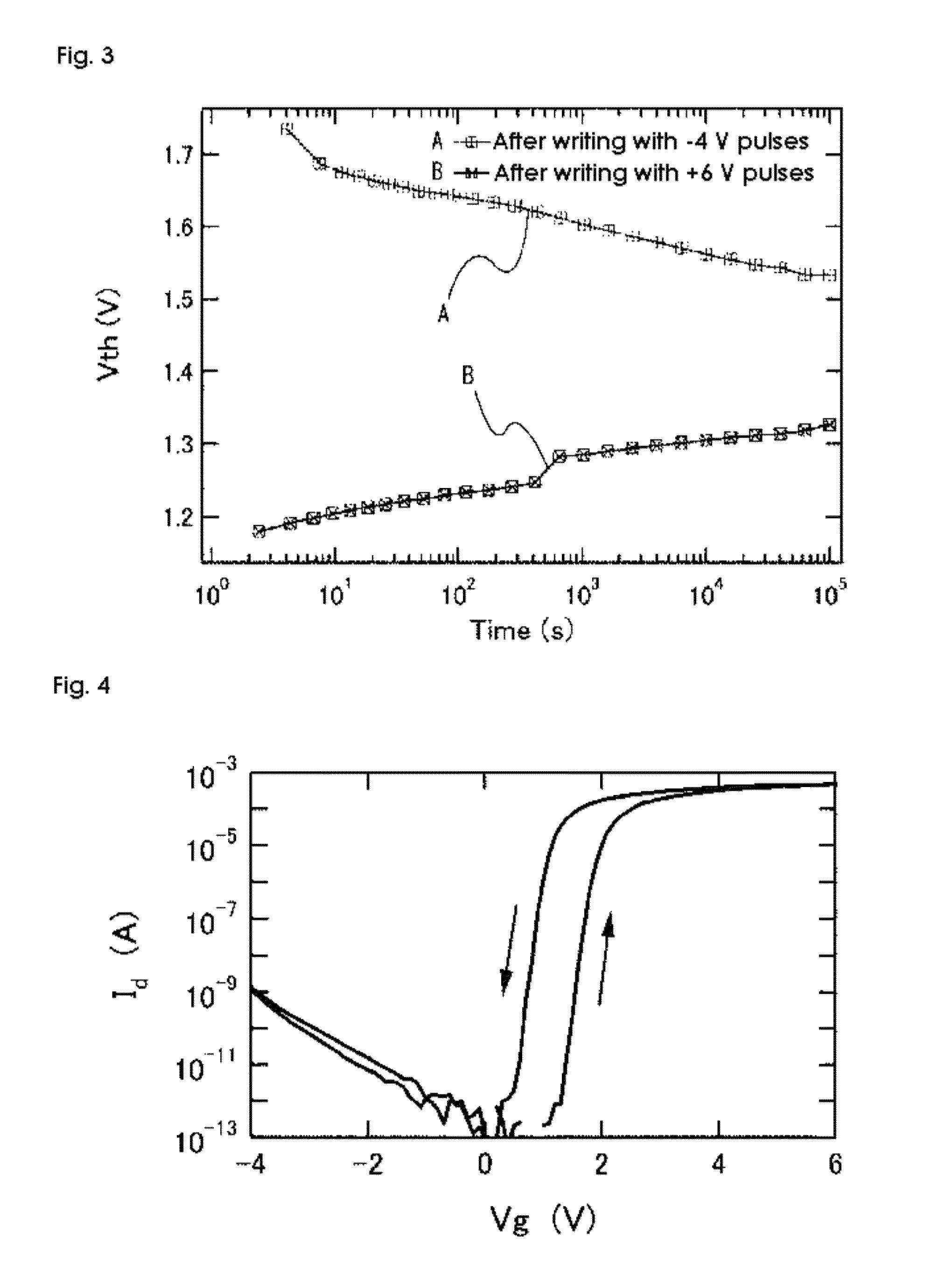
[0291]FIG. 4 shows Id−Vg characteristics. Measurement as is that in FIG. 2 is made in which the gate voltage is swept in reciprocation between −4 and 6 V. At Id=2×10⁻⁶ A, a memory window of 0.84 V is had.

example 3

[0292]In this Example, a substrate temperature different from those in Examples 1 and 2 is used. Also, the rates of flow of MOCVD liquid materials and the period of heat treatment for crystallization are altered. Also, the time period of heat treatment for crystallization is 1 hour. Other conditions are identical to those in Example 1. To wit:

[0293]Substrate Temperature: 450° C.

[0294]Liquid Raw Materials

[0295]ST-1 (concentration of 0.1 M): 0.097 sccm

[0296]CT-1 (concentration of 0.1 M): 0.032 sccm

[0297]Bi (MMP)3: (concentration of 0.2 M): 0.140 sccm

[0298]PET (concentration of 0.1 M): 0.032 sccm

[0299]Film Forming Time Period: 1940 seconds

[0300]Heat Treatment Conditions: heat treatment in oxygen under the atmospheric pressure, at a temperature of 800° C. and for a time period of 30 minutes.

[0301]FIG. 5 shows Id−Vg characteristics. Measurement as is that in FIG. 2 is made in which the gate voltage is swept in reciprocation between −4 and 6 V. At Id=2×10⁻⁶ A, a memory window of 0.75 V is...


PUM

PropertyMeasurementUnit
Lengthaaaaaaaaaa
Thicknessaaaaaaaaaa
Thicknessaaaaaaaaaa

Abstract

A ferroelectric device and a manufacturing method are provided. While holding a nonvolatile memory retention capability and a multiple rewriting endurance as the distinctive features of a ferroelectric device, the disclosed ferroelectric device is wider in memory window and more adaptively made microfiner than a conventional ferroelectric device that has used a ferroelectric mainly constituted of Sr—Bi—Ta—O as an oxide of strontium, bismuth and tantalum. Directly on or with intermediary of an insulator on a semiconductor there are layered a first ferroelectric and a conductor to form a gate stack, the first ferroelectric being mainly constituted of Sr—Ca—Bi—Ta—O as an oxide of strontium, calcium, bismuth and tantalum and being built up by a metal organic vapor deposition technique from a suitable film-forming raw material. The gate stack is heat-treated to cause the first ferroelectric to develop its ferroelectricity.

Description

TECHNICAL FIELD[0001]The present invention relates to a ferromagnetic device and a method of its manufacture. The invention is concerned with a ferroelectric device such as, e. g., a semiconductor transistor in which its gate insulator film is constituted as a multi-layered structure including a ferroelectric, as well as to a method of making such devices.BACKGROUND ART[0002]A transistor using a ferroelectric for its gate insulator film which allows data storage and data reading and writing to be conducted by the single transistor is expected to be a highly integrated memory in the next generation. Transistors of this type have their electrical conduction controlled corresponding to directions of the electric polarization of a ferroelectric. While their prototype is an MFS transistor having an MFS (metal, ferroelectric and semiconductor) laminated structure, a structure is also being investigated in which so that both characteristics of the semiconductor and ferroelectric may not be...

Claims


Application Information

Patent Timeline
IPC IPC(8): H01L29/78H01L21/28H01L29/66
CPCC23C16/40H01L21/28291H01L29/516H01L21/02271H01L27/1159H01L29/78391H01L21/02197H01L29/6684H01L29/40111H10B51/30
Inventor SAKAI, SHIGEKITAKAHASHI, MITSUEKUSUHARA, MASAKITODA, MASAYUKIUMEDA, MASARU
Owner NAT INST OF ADVANCED IND SCI & TECH
Why Eureka
Try Eureka