Electron beam masks for compressive sensors

a technology of compressive sensor and electron beam, which is applied in the direction of microlithography exposure apparatus, electric discharge tube, diaphragm/collimeter handling, etc., can solve the problems of image read-out, many challenges associated with capturing dynamic processes with high temporal resolution,

Active Publication Date: 2016-09-22
BATTELLE MEMORIAL INST
View PDF29 Cites 4 Cited by
  • Summary
  • Abstract
  • Description
  • Claims
  • Application Information

AI Technical Summary

Problems solved by technology

While many developments in electron optics and the design of in-situ cells have been made, leading to significant improvements in achievable resolution, there are still many challenges associated with capturing dynamic processes with high temporal resolution.
While improving temporal resolution, DDCs can also enable electron dose reduction, another challenge for in-situ TEM imaging.
A potential limitation is that as frame rates increase, image read-out can become a challenge due to the increased data rates.

Method used


Image

  • Electron beam masks for compressive sensors
  • Electron beam masks for compressive sensors
  • Electron beam masks for compressive sensors

Examples


example 1

Charged Particle Beam Imaging System

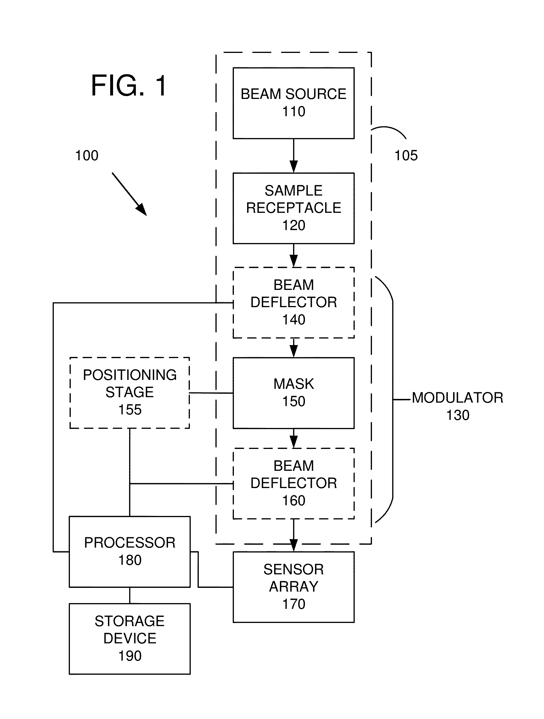
[0060]FIG. 1 illustrates a representative charged particle beam (CPB) imaging system 100. It should be noted that FIG. 1 and the other Figures herein are provided for illustrative purposes and are not to proportion or to scale unless specifically noted as being to scale. The CPB imaging system 100 include a CPB column 105 for forming and transforming a charged particle beam that is directed toward a sensor array 170. The column 105 includes various CPB optical components, such as one or more of beam sources, lenses, apertures, deflection systems, alignment coils, blanking plates, scintillators, and stigmators. As shown in FIG. 1, the column 105 includes a beam source 110 that directs a beam toward sample that is retained by a sample receptacle 120. A modulator 130 is situated between the sample and the sensor array 170 so as to apply a modulation to a transmitted CPB image beam. The column 105 is generally coupled to a vacuum pump and one or more ...

example 2

Charged Particle Beam CS Methods

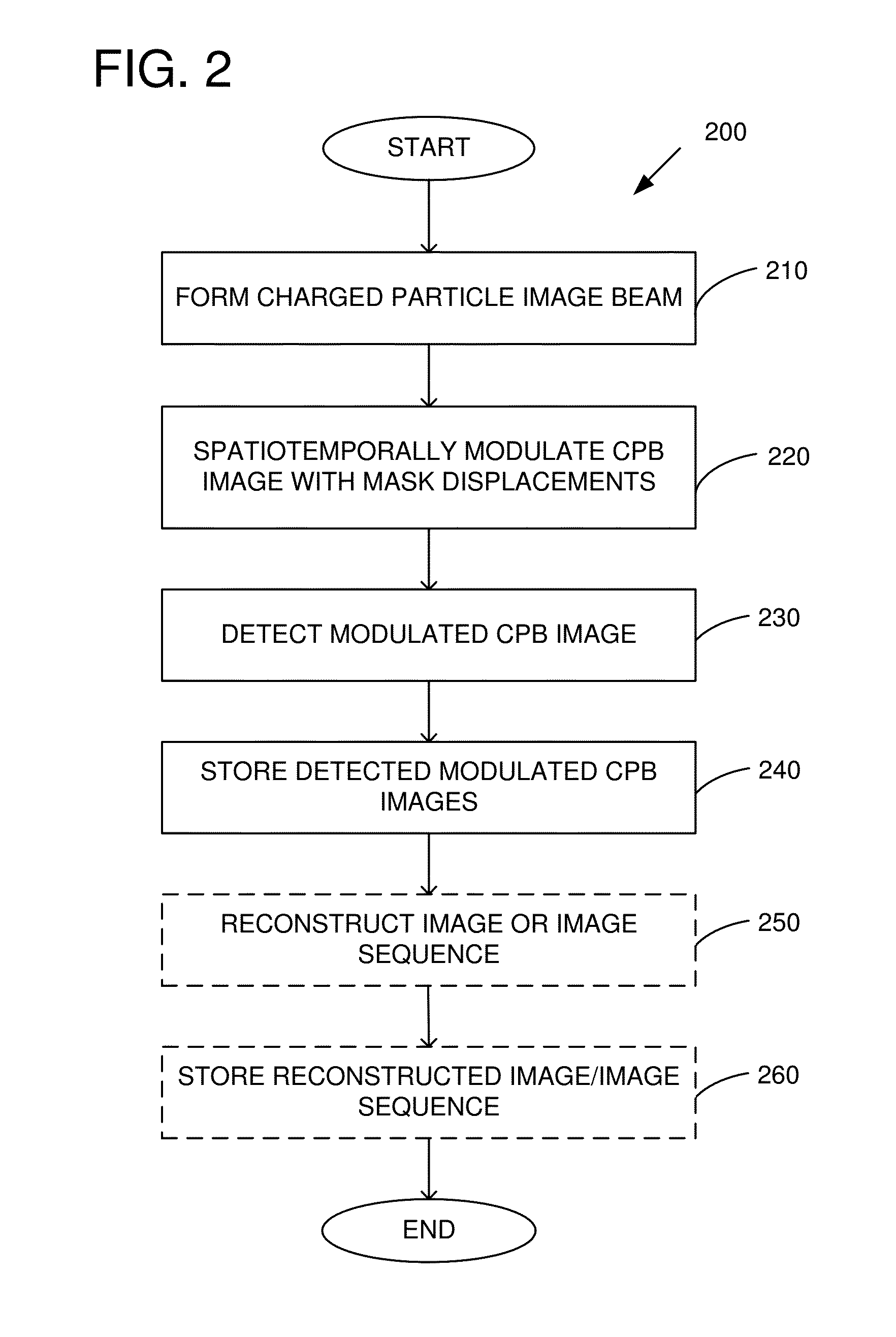
[0066]FIG. 2 illustrates an example method 200 for CPB imaging using CS. Such a method can be implemented using various CPB imaging systems such as, for example, the imaging system shown in FIG. 1. At 210, a charged particle (CP) image beam is formed by, for example, exposing a sample to a CPB such as an electron or ion beam. As a specific example, the CPB beam can be transmitted through the sample to form the CP image beam. Variations in intensity or phase in the CP image beam are associated with differences in structure and / or composition of the sample. At 220, the image beam can be spatiotemporally modulated using displacement of the CP image beam with respect to a mask. The CP image beam can be modulated in a variety of ways including by moving a mask with respect to the CP image beam and / or by moving or scanning the CP image beam relative to the aperture. As one example, the beam is modulated by mechanically moving the mask using a translation or...

example 3

Charged Particle Beam Microscopy System

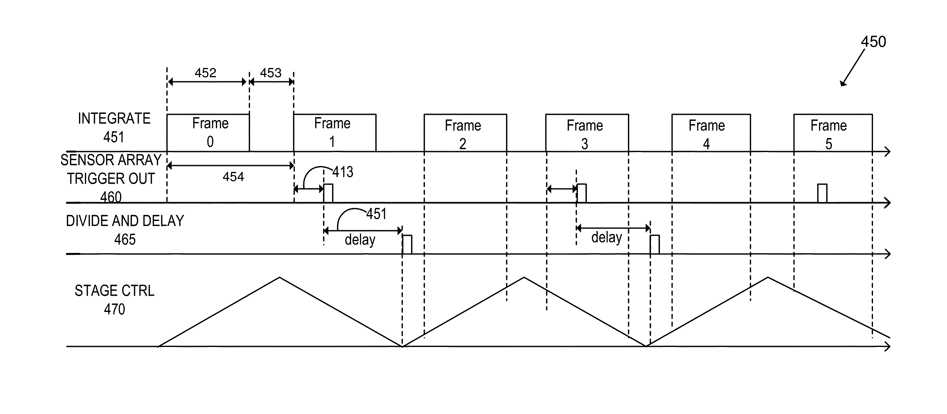
[0072]A representative CPB microscopy system 300 using a stationary beam and a moving aperture is illustrated in FIG. 3. A CPB source 310 directs a CPB 315 to a specimen 320 so as to produce an image beam 325. A positioning stage 355 is coupled to a mask 350 that is scanned with respect to the image beam 325 to produce a mask-modulated image beam 340. A sensor array 370 receives the mask-modulated image beam 340 and integrates for a time duration established by a controller 380, or otherwise determined. Detected images are stored in a memory 390. For continuous detection of the modulated image beam, an integration time can be less than or equal to a frame time (a reciprocal of the frame rate). For example, one image can be collected while a previous captured image is scanned out of the sensor array 370.

[0073]The microscopy system 300 can include sensor arrays of various sizes and resolutions. For example the sensor array 370 can have an array 5...


PUM

PropertyMeasurementUnit
thicknessaaaaaaaaaa
thicknessaaaaaaaaaa
transmittanceaaaaaaaaaa

Abstract

Transmission microscopy imaging systems include a mask and / or other modulator situated to encode image beams, e.g., by deflecting the image beam with respect to the mask and / or sensor. The beam is modulated / masked either before or after transmission through a sample to induce a spatially and / or temporally encoded signal by modifying any of the beam / image components including the phase / coherence, intensity, or position of the beam at the sensor. For example, a mask can be placed / translated through the beam so that several masked beams are received by a sensor during a single sensor integration time. Images associated with multiple mask displacements are then used to reconstruct a video sequence using a compressive sensing method. Another example of masked modulation involves a mechanism for phase-retrieval, whereby the beam is modulated by a set of different masks in the image plane and each masked image is recorded in the diffraction plane.

Description

CROSS REFERENCE TO RELATED APPLICATIONS[0001]This application claims the benefit of U.S. Provisional Application No. 62 / 134,932, entitled “COMPRESSIVE TRANSMISSION ELECTRON MICROSCOPY,” filed Mar. 18, 2015, and U.S. Provisional Application No. 62 / 148,619, entitled “COMPRESSIVE TRANSMISSION ELECTRON MICROSCOPY,” filed Apr. 16, 2015. The entire disclosures of both applications are incorporated herein by reference.ACKNOWLEDGMENT OF GOVERNMENT SUPPORT[0002]This invention was made with government support under grants DE-FG02-03ER46057 and DE-AC05-76RL01830 awarded by the United States Department of Energy. The government has certain rights in the invention.BACKGROUND[0003]In-situ transmission electron microscopy (TEM) can be a powerful analytical technique for enabling insight into the nature of materials under a broad range of environmental conditions. With the development of a wide range of in-situ TEM stages and dedicated environmental TEM, it is possible to image materials under high...

Claims


Application Information

Patent Timeline
Patent Type & Authority Applications(United States)
IPC IPC(8): G21K1/02G03F7/30G03F7/20
CPCG21K1/02G03F7/30G03F7/20H01J2237/0453H01J2237/226H01J2237/24455H01J2237/2802H01J37/244H01J37/222H01J37/26H01J2237/0451
Inventor STEVENS, ANDREW J.KOVARIK, LIBORBROWNING, NIGEL D.LIYU, ANDREY V.
Owner BATTELLE MEMORIAL INST
Why Eureka
Try Eureka