Patch antenna

a technology of patch antenna and ebg structure, which is applied in the direction of individual energised antenna arrays, resonant antennas, substantially flat resonant elements, etc., can solve the problems of difficult to reduce the size of the antenna including the cavity, difficult to reduce the size of the antenna including the ring mushroom structure, and difficult to reduce the size of the antenna including the ebg structure. , to achieve the effect of suppressing the generation of surface waves,

Active Publication Date: 2016-09-22
MURATA MFG CO LTD
View PDF1 Cites 20 Cited by
  • Summary
  • Abstract
  • Description
  • Claims
  • Application Information

AI Technical Summary

Benefits of technology

[0017]An object of the present disclosure is to provide an antenna device that suppresses the generation of a surface wave and that is suited for miniaturization.
[0025]The inclusion of the cavity can suppress generation of a surface wave. The inclusion of the reactance component in the impedance that the side face of the cavity exhibits can avoid a narrowed band resulting from the inclusion of the cavity. Because it is not necessary to cause the cavity and radiation electrode to resonate with each other, flexibility in the dimensions of the cavity is enhanced, and the size of the cavity can be reduced.
[0026]A resonant frequency of the cavity may preferably be higher than a resonant frequency of the radiation electrode. An increased resonant frequency of the cavity can lead to a reduced size in the cavity.
[0030]The at least one linear conductor in the reactance element may include a plurality of linear conductors disposed in different locations in a thickness direction of the dielectric substrate. In this configuration, flexibility in adjustment of reactance that the side face of the cavity exhibits can be enhanced.
[0031]The linear conductor may include a portion that extends in a direction that crosses a shortest route from a place where the linear conductor is connected to the side face of the cavity to the radiation electrode as seen in a plan view. Because the shortest distance between the radiation electrode and the linear conductor is increased, degradation of antenna characteristics resulting from capacitive coupling can be suppressed.
[0032]The inclusion of the cavity can suppress generation of a surface wave. The inclusion of the reactance component in the impedance that the side face of the cavity exhibits can avoid a narrowed band resulting from the inclusion of the cavity. Because it is not necessary to cause the cavity and radiation electrode to resonate with each other, flexibility in the dimensions of the cavity can be enhanced, and the size of the cavity can be reduced.

Problems solved by technology

Because the dimensions of the cavity depend on the operating frequency band, it is difficult to reduce the size of the antenna including the cavity.
Thus, it is difficult to reduce the size of the antenna including the ring mushroom structure.
Thus, it is difficult to reduce the size of the antenna including the EBG structure.

Method used


Image

  • Patch antenna
  • Patch antenna
  • Patch antenna

Examples


first embodiment

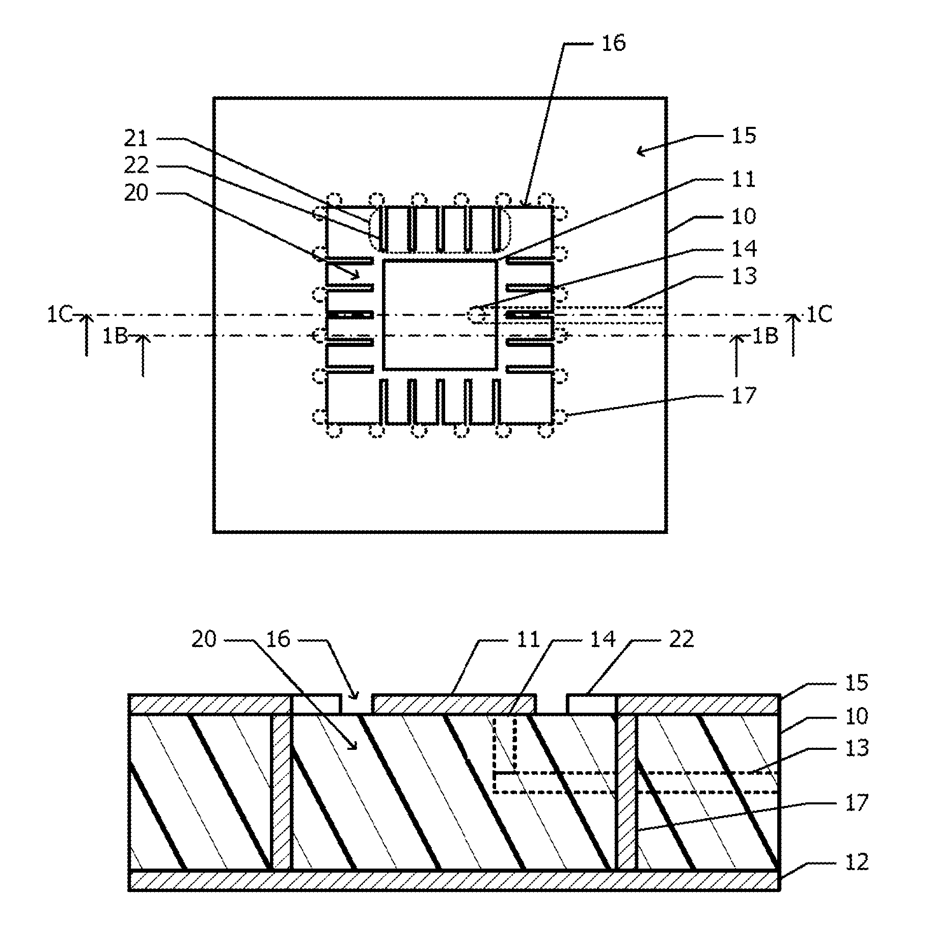
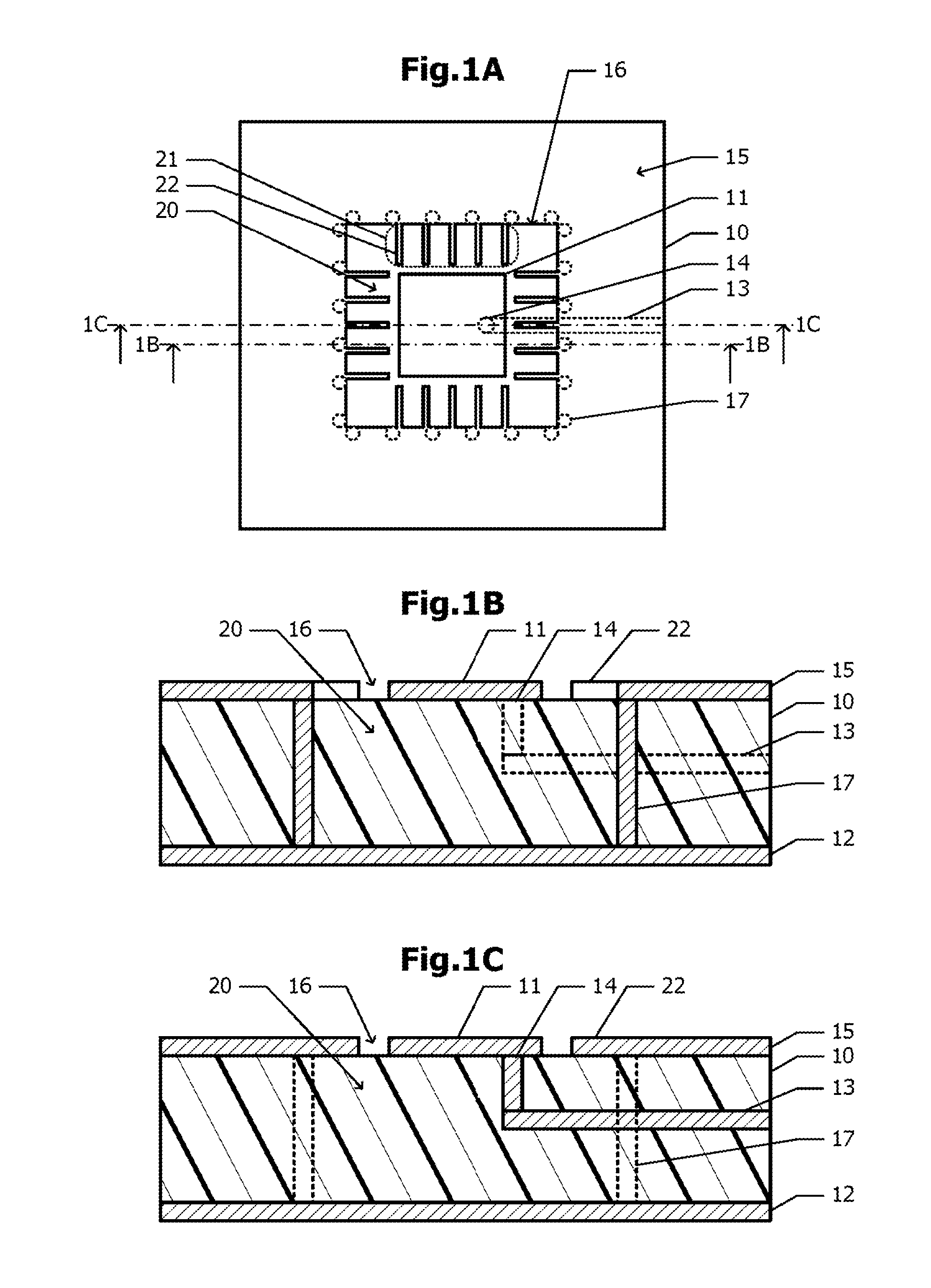
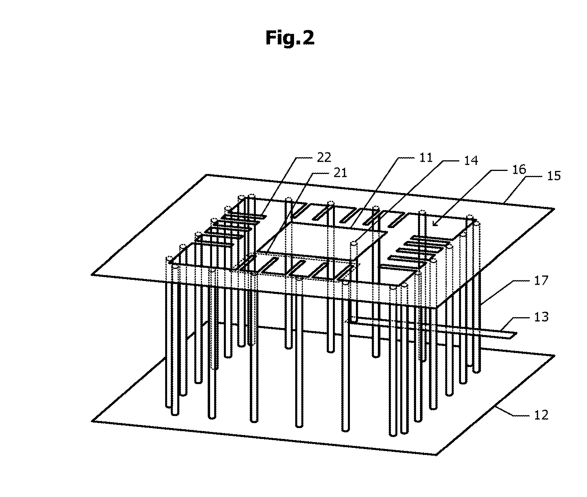
[0042]FIG. 1A is a plan view of a patch antenna according to a first embodiment. FIGS. 1B and 1C are cross-sectional views taken along dot-dash lines 1B-1B and 1C-1C in FIG. 1A, respectively. FIG. 2 is a perspective view of the patch antenna according to the first embodiment.

[0043]A radiation electrode 11 and a surface-layer conductive plate 15 are disposed on a surface of a dielectric substrate 10. The surface-layer conductive plate 15 has an opening 16. The radiation electrode 11 is disposed inside the opening 16. The surface where the radiation electrode 11 and the surface-layer conductive plate 15 are disposed is referred to as “first surface.” A surface opposite to the first surface is referred to as “second surface.” A ground conductive plate 12 is disposed on the second surface of the dielectric substrate 10. An example planar shape of each of the radiation electrode 11 and opening 16 may be a square or rectangle. The edges of the radiation electrode 11 and the edges of the o...

second embodiment

[0052]Next, a patch antenna according to a second embodiment is described with reference to FIGS. 3A to 3C. Differences from the patch antenna according to the first embodiment illustrated in FIGS. 1A to 2 are described below, and the description about the same configurations is omitted.

[0053]FIG. 3A is a plan view of the patch antenna according to the second embodiment. FIGS. 3B and 3C are cross-sectional views taken along dot-dash lines 3B-3B and 3C-3C in FIG. 3A, respectively. In the first embodiment, no other conductive plates are disposed between the ground conductive plate 12 and surface-layer conductive plate 15 (FIGS. 1B and 1C). In the second embodiment, as illustrated in FIGS. 3B and 3C, other inner-layer conductive plates 25 and 26 are disposed between the ground conductive plate 12 and surface-layer conductive plate 15.

[0054]Each of the inner-layer conductive plates 25 and 26 has the same planar shape as that of the surface-layer conductive plate 15. That is, the inner-l...

third embodiment

[0056]A patch antenna according to a third embodiment is described with reference to FIGS. 4A and 4B. Differences from the patch antenna according to the first embodiment illustrated in FIGS. 1A to 2 are described below, and the description about the same configurations is omitted.

[0057]FIGS. 4A and 4B are cross-sectional views taken along the dot-dash lines 1B-1B and 1C-1C in FIG. 1A, respectively. In the third embodiment, an inner-layer conductive plate 25 and linear conductors 29 are added. The inner-layer conductive plate 25 and linear conductors 29 have the same configurations as those of the inner-layer conductive plate 25 and linear conductors 29 in the patch antenna according to the second embodiment illustrated in FIGS. 3B and 3C.

[0058]The radiation electrode 11 in the patch antenna according to the third embodiment has a stacking structure including a passive electrode 11A and a feeding electrode 11B. The passive electrode 11A has the same planar shape as that of the radia...


PUM


Abstract

A surface-layer conductive plate having an opening is disposed on a first surface of a dielectric substrate. A radiation electrode is disposed inside the opening on the first surface of the dielectric substrate. A ground conductive plate is disposed on a second surface of the dielectric substrate, the second surface being opposite to the first surface. Interlayer connection members are disposed so as to surround the opening as seen in a plan view. The interlayer connection members electrically connects the surface-layer conductive plate to the ground conductive plate and defines a cavity that causes electromagnetic resonance to occur. A reactance element is configured to cause an impedance that a side face of the cavity exhibits with respect to an electromagnetic wave propagating in the cavity to include a reactance component.

Description

BACKGROUND OF THE DISCLOSURE[0001]1. Field of the Disclosure[0002]The present disclosure relates to a patch antenna including a radiation electrode and a cavity.[0003]2. Description of the Related Art[0004]In a patch antenna in which a ground conductor plate is disposed on one surface of a dielectric substrate and a radiation electrode is disposed on another surface, the use of a high permittivity substrate can achieve size reduction in the antenna. When the permittivity of the dielectric substrate is increased, the band width becomes narrow and the possibility of generation of an electromagnetic wave (surface wave) propagating in an in-plane direction in the dielectric substrate is increased. When the surface wave is generated, a radiation pattern of the patch antenna is deformed and a gain in a desired direction is decreased.[0005]Increasing the thickness of the dielectric substrate can widen the band width. However, when the thickness of the dielectric substrate is increased, the...

Claims


Application Information

Patent Timeline
Patent Type & Authority Applications(United States)
IPC IPC(8): H01Q21/06H01Q9/04H01Q1/48
CPCH01Q21/065H01Q9/0442H01Q1/48H01Q1/38H01Q9/0421H01Q9/0407H01Q9/0414H01Q19/10H01Q5/378
Inventor UEDA, HIDEKI
Owner MURATA MFG CO LTD
Why Eureka
Try Eureka