Semiconductor device and method of manufacturing the same
- Summary
- Abstract
- Description
- Claims
- Application Information
AI Technical Summary
Benefits of technology
Problems solved by technology
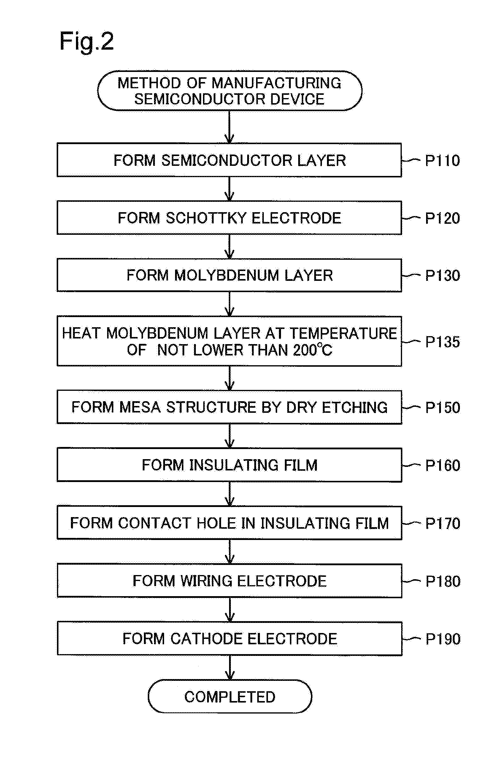
Method used
Image

Examples
first embodiment
A. First Embodiment
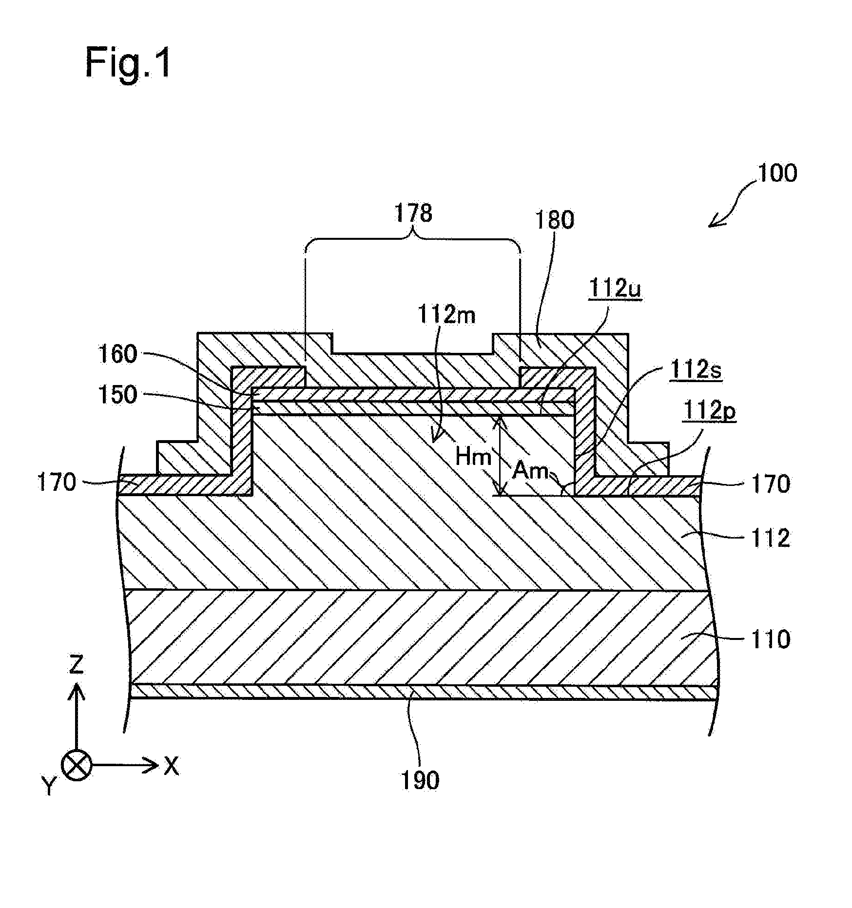
[0051]A-1. Configuration of Semiconductor Device
[0052]FIG. 1 is a sectional view schematically illustrating the configuration of a semiconductor device 100 according to a first embodiment. XYZ axes orthogonal to one another are illustrated in FIG. 1. Among the XYZ axes of FIG. 1, the X axis denotes a left-right axis on the sheet surface of FIG. 1. +X-axis direction denotes a rightward direction on the sheet surface, and −X-axis direction denotes a leftward direction on the sheet surface. Among the XYZ axes of FIG. 1, the Y axis denotes a front-back axis on the sheet surface of FIG. 1. +Y-axis direction denotes a backward direction on the sheet surface, and −Y-axis direction denotes a forward direction on the sheet surface. Among the XYZ axes of FIG. 1, the Z axis denotes a top-bottom axis on the sheet surface of FIG. 1. +Z-axis direction denotes an upward direction on the sheet surface, and −Z-axis direction denotes a downward direction on the sheet surface. The X...
second embodiment
B. Second Embodiment
[0091]B-1. Configuration of Semiconductor Device
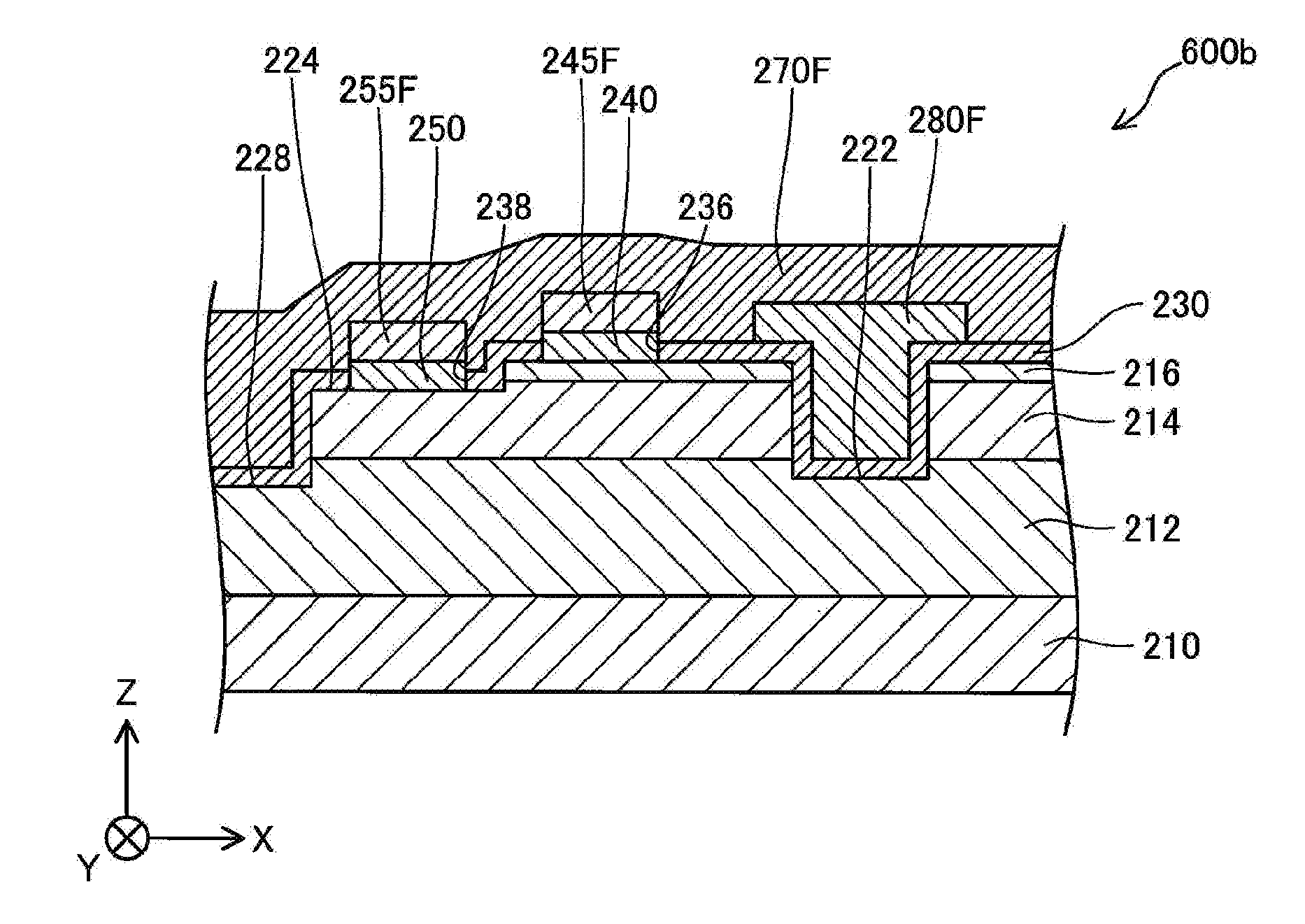
[0092]FIG. 9 is a sectional diagram schematically illustrating the configuration of a semiconductor device 200 according to a second embodiment. XYZ axes orthogonal to one another are illustrated in FIG. 9, like FIG. 1.
[0093]The semiconductor device 200 is a GaN-based semiconductor device formed using gallium nitride (GaN). According to this embodiment, the semiconductor device 200 is a vertical trench MOSFET (metal-oxide-semiconductor field effect transistor). According to this embodiment, the semiconductor device 200 is used for power control and is also called power device.
[0094]The semiconductor device 200 includes a substrate 210, a semiconductor layer 212, a semiconductor layer 214 and a semiconductor layer 216. The semiconductor device 200 has a trench 222, a recess 224 and a trench 228 as structures formed in these semiconductor layers. The semiconductor device 200 also includes an insulating film 230, a sou...
third embodiment
C. Third Embodiment
[0138]FIG. 17 is a sectional view schematically illustrating the configuration of a semiconductor device 300 according to a third embodiment. The configuration of the semiconductor device 300 is similar to the configuration of the semiconductor device 200 of the second embodiment, except that a source electrode 240C is provided in place of the source electrode 240 and that a molybdenum layer 245C is provided in place of the molybdenum layers 245 and 255.
[0139]The source electrode 240C of the semiconductor device 300 is similar to the source electrode 240 of the second embodiment, except that the source electrode 240C is formed from inside of the contact hole 236 over the body electrode 250. The molybdenum layer 245C of the semiconductor layer 300 is similar to the molybdenum layers 245 and 255 of the second embodiment except that the molybdenum layer 245C is formed on the source electrode 240C to cover the body electrode 250 via the source electrode 240C. This con...
PUM
 Abstract
Description
Claims
Application Information
 - R&D Engineer
- R&D Manager
- IP Professional
- Industry Leading Data Capabilities
- Powerful AI technology
- Patent DNA Extraction
Browse by: Latest US Patents, China's latest patents, Technical Efficacy Thesaurus, Application Domain, Technology Topic.
© 2024 PatSnap. All rights reserved.Legal|Privacy policy|Modern Slavery Act Transparency Statement|Sitemap